Previous: 4.2.1 Introduction Up: 4.2 Lateral Trench Gate SOI-LDMOSFETs Next: 4.2.3 Simulation Results
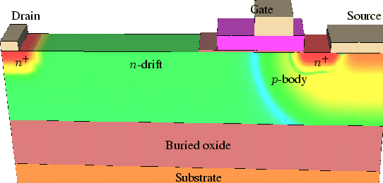
Figure 4.12 and Figure 4.13 show the schematic structures of a conventional LDMOSFET on SOI and a proposed lateral trench gate SOI-LDMOSFET, which are used for the simulation of the BV and on-resistance, respectively. Generally, the BV of conventional SOI-LDMOSFETs is limited by the buried oxide thickness, SOI thickness, and the drift layer length. Most of the voltage drops over the buried oxide layer, and the maximum electric field at the interface between silicon and the buried oxide is limited by that of the silicon region at the interface. To obtain a higher breakdown voltage with thick film SOI-LDMOSFETs, the buried oxide or the SOI layer thickness must be increased.
Figure 4.12 shows a conventional
![]() -channel SOI-LDMOSFET designed for a BV of 100V
with an SOI thickness
-channel SOI-LDMOSFET designed for a BV of 100V
with an SOI thickness
![]() of 1.5
of 1.5![]() m and a buried
oxide thickness
m and a buried
oxide thickness
![]() of 1.0
of 1.0![]() m.
The drift region of the device is doped according to the
RESURF principle.
To obtain a better trade-off between the BV and the on-resistance a
highly doped
m.
The drift region of the device is doped according to the
RESURF principle.
To obtain a better trade-off between the BV and the on-resistance a
highly doped ![]() -buffer is added at the drain.
The on-resistance of the low and medium voltage devices is
determined by the drift and channel resistance. To achieve a
lower on-resistance the drift doping or the channel area must
be increased. The drift doping, however, is limited by
the RESURF condition, and the channel area affects the chip size.
-buffer is added at the drain.
The on-resistance of the low and medium voltage devices is
determined by the drift and channel resistance. To achieve a
lower on-resistance the drift doping or the channel area must
be increased. The drift doping, however, is limited by
the RESURF condition, and the channel area affects the chip size.
 |
Figure 4.13 shows the proposed lateral
trench gate SOI-LDMOSFET and the current flow iso-lines at
![]()
![]() 12V and
12V and
![]()
![]() 2.0V. As shown in the figure,
the proposed device structure is similar to
that of a conventional SOI-LDMOSFET except that
it has a trench gate on the side wall.
Together with the channel on the top of the SOI this gives an
increased channel area, and an effective
2.0V. As shown in the figure,
the proposed device structure is similar to
that of a conventional SOI-LDMOSFET except that
it has a trench gate on the side wall.
Together with the channel on the top of the SOI this gives an
increased channel area, and an effective ![]() -drift area (near the
gate edge) which contributes to current conduction during
on-state, is increased. From Figure 4.13 it is clear that the
channel current flows on the side wall of the trench. With
the increased channel area and the effective n-drift area
a reduction of the on-resistance can be achieved.
-drift area (near the
gate edge) which contributes to current conduction during
on-state, is increased. From Figure 4.13 it is clear that the
channel current flows on the side wall of the trench. With
the increased channel area and the effective n-drift area
a reduction of the on-resistance can be achieved.
The trench depth and the space between the trench determine the
channel area of the device.
The width, space, and depth of the lateral trench gate are
0.4![]() m, from 0.5 to 1.1
m, from 0.5 to 1.1![]() m, and from 0.5 to 1.5
m, and from 0.5 to 1.5![]() m,
respectively. Simulations are performed for the 100V lateral
trench gate SOI-LDMOSFETs with an
m,
respectively. Simulations are performed for the 100V lateral
trench gate SOI-LDMOSFETs with an ![]() -drift length
-drift length
![]()
![]() 5.5
5.5![]() m and doping
m and doping
![]()
![]() 1.0
1.0 ![]()
![]()
![]() .
The other structure parameters are the same as that
in Figure 4.12.
Table 4.1 shows the technological and geometrical
parameters considered for device analysis.
.
The other structure parameters are the same as that
in Figure 4.12.
Table 4.1 shows the technological and geometrical
parameters considered for device analysis.
| Parameter | Value |
| 1.0 |
|
| 5.5 |
|
| SOI thickness
|
1.5 |
| 5.0 |
|
| Buried oxide thickness
|
1.0 |
| Lateral trench gate width | 0.4 |
| Lateral trench gate space | 0.5 - 1.1 |
| Lateral trench gate depth | 0.5 - 1.5 |