Previous: 4.5.1 Introduction Up: 4.5 Shorted-Anode LIGBT on SOI with Trench Oxide Next: 4.5.3 Simulation Results
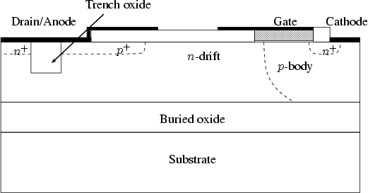
Figure 4.43 shows the schematic structure of the proposed SOI SA-LIGBT.
The ![]() -layer is introduced to the
-layer is introduced to the ![]() -anode region to achieve a
shorted-anode structure. As can be seen in the figure, the
-anode region to achieve a
shorted-anode structure. As can be seen in the figure, the ![]() -
and
-
and ![]() -areas are separated by the trench oxide.
-areas are separated by the trench oxide.
The device is designed to achieve a BV of 120V with an SOI thickness
![]() of 2.0
of 2.0![]() m and with a buried oxide thickness
m and with a buried oxide thickness
![]() of 1.0
of 1.0![]() m.
The design parameters used for this analysis are listed in Table 4.5.
m.
The design parameters used for this analysis are listed in Table 4.5.
The maximum BV of the SOI SA-LIGBT is limited by the thickness of
the buried oxide. An optimal drift length and doping must be
ensured to get the best trade-off between the on-resistance and the BV.
As shown in the table the ![]() -drift length is 8.5
-drift length is 8.5![]() m, the doping
amounts to 1.0
m, the doping
amounts to 1.0 ![]()
![]()
![]() , and the trench oxide depth
is 1.0
, and the trench oxide depth
is 1.0![]() m. A highly doped
m. A highly doped ![]() -buffer is added at the drain/anode
region which helps to prevent punch through at this region.
-buffer is added at the drain/anode
region which helps to prevent punch through at this region.
To suppress the NDR
the length of the ![]() -anode of the conventional SA-LIGBT must
be increased. To overcome this drawback we introduce a trench
oxide at the drain/anode region. The
-anode of the conventional SA-LIGBT must
be increased. To overcome this drawback we introduce a trench
oxide at the drain/anode region. The ![]() -drain length of 2.0
-drain length of 2.0![]() m
and the
m
and the ![]() -anode length of 6.0
-anode length of 6.0![]() m are used through out all the
simulations.
With the structure proposed it is possible to suppress the NDR
without increasing the
m are used through out all the
simulations.
With the structure proposed it is possible to suppress the NDR
without increasing the ![]() -anode length.
-anode length.
As shown in Figure 4.43, the device has a hybrid LDMOSFET-LIGBT structure
with a common drift region.
The ![]() -anode provides conductivity modulation of the
-anode provides conductivity modulation of the ![]() -drift region.
The
-drift region.
The ![]() -drain defines a lateral DMOS structure and an electron extraction
path during turn-off of the device.
As a result two different modes of on-state operation can be seen,
which depend on the bias conditions.
-drain defines a lateral DMOS structure and an electron extraction
path during turn-off of the device.
As a result two different modes of on-state operation can be seen,
which depend on the bias conditions.
At low anode voltages the device exhibits MOSFET operation.
Only the ![]() -region at the drain/anode contributes to the current conduction
in the on-state and significant conductivity modulation of the
-region at the drain/anode contributes to the current conduction
in the on-state and significant conductivity modulation of the ![]() -drift
region cannot be seen. As the anode voltage increases, the potential
underneath the
-drift
region cannot be seen. As the anode voltage increases, the potential
underneath the ![]() -anode starts to fall and makes
the
-anode starts to fall and makes
the ![]() -anode and
-anode and ![]() -drift junction forward biased. Considerable
injection of holes from the
-drift junction forward biased. Considerable
injection of holes from the ![]() -anode to the
-anode to the ![]() -drift region takes place,
resulting in a lower forward voltage drop than that of the SOI-LDMOSFET.
Figure 4.44 shows the current flow of the proposed SA-LIGBT
at
-drift region takes place,
resulting in a lower forward voltage drop than that of the SOI-LDMOSFET.
Figure 4.44 shows the current flow of the proposed SA-LIGBT
at
![]()
![]() 12V and
12V and
![]()
![]() 10V. The electron current at the
10V. The electron current at the
![]() drain region, and the hole current at the
drain region, and the hole current at the ![]() -anode and
under the cathode (
-anode and
under the cathode (![]() -body region) can be seen simultaneously.
-body region) can be seen simultaneously.
Jong-Mun Park 2004-10-28