|
|
|
|
Dissertation Christian Poschalko | Previous: 3.2 Direct radiation from PCB sources Up: 3.2 Direct radiation from PCB sources Next: 3.2.2 Direct radiation from plane edges on the |
|
|
|
|
Dissertation Christian Poschalko | Previous: 3.2 Direct radiation from PCB sources Up: 3.2 Direct radiation from PCB sources Next: 3.2.2 Direct radiation from plane edges on the |
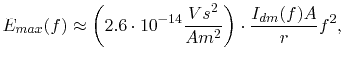
According to [58] the estimation for the maximum radiated electric far field density from a loop current Idm on a PCB as depicted in Figure 3.1 is
C. Poschalko: The Simulation of Emission from Printed Circuit Boards under a Metallic Cover
![\includegraphics[height=4 cm,viewport=70 590 540
720,clip]{pics/Abstrahlung_Schleife.eps}](img216.png)