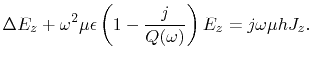
Figure 4.1 depicts a cross-section of the volume between a PCB
ground plane and a metallic cover. This volume contains the metallic layout structures on
the PCB, the active and passive components, metallic cooling structures, thin sheets of
PCB dielectric material, and for the most part air. In case of a PCB stack the metallic
cover plane is given by the ground plane of the parallel PCB.
Figure 4.1:
Cross-section of the volume between the PCB ground plane and the metallic
enclosure cover.
|
![\includegraphics[width=13.5cm,viewport=50 540 500
750,clip]{{pics/PCB_Cover_Content.eps}}](img230.png) |
All metallic PCB layout structures, the components on the PCB, and metallic cooling
devices will be introduced into the field formulation by excitation ports in a second
step and, thus, these parts are neglected for the derivation of the cavity field
equation. Therefore, the field is derived for a volume that contains only isolating
dielectric layers. The first and the third Maxwell equations for harmonic signals
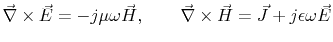 |
(4.1) |
are combined to
 |
(4.2) |
Where  is the electrical field strength,
  is the current density,
 is the permittivity of the layer,
  is the permeability of the layer and
 , with the frequency f.
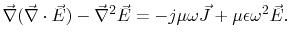
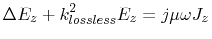
The dielectric layers of such applications (air, FR4,...) are usually homogenous
regarding their macroscopic electrical parameters. Therefore, there are no charges
(
 ) inside one layer and the first term
of (4.2) vanishes, leading to the three-dimensional,
vectorial Helmholtz equation
) inside one layer and the first term
of (4.2) vanishes, leading to the three-dimensional,
vectorial Helmholtz equation
 |
(4.3) |
Equation (4.3) is general for homogenous materials without
volume charges. It can be reduced to a scalar two-dimensional Helmholtz equation by the
following conditions:
Perfect conducting cover and ground plane: 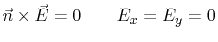 |
(4.4) |
Electrically small cover to ground plane distance: |
(4.5) |
Condition (4.4) is reasonable for emission simulation of
enclosures, because the main loss mechanism is the radiation loss from the enclosure
slots, which dominates compared to the conduction loss of the metallic planes
[45]. However, conduction and dielectric losses will be considered in the
cavity model, without noticeable violation of the condition.
Condition (4.5) limits the frequency range for the model.
Table 4.1 list the frequency limits for some cover to ground plane
distances based on the often used
 lumped element criterion and the more
tolerable
lumped element criterion and the more
tolerable
 condition for short antennas. The table demonstrates that the
whole CISPR25 frequency range of 2.5GHz is covered up to a plane separation of 15mm and
nearly covered up to 20mm. The maximum frequency limit is beyond 1 GHz even at a plane
separation distance of 30mm.
condition for short antennas. The table demonstrates that the
whole CISPR25 frequency range of 2.5GHz is covered up to a plane separation of 15mm and
nearly covered up to 20mm. The maximum frequency limit is beyond 1 GHz even at a plane
separation distance of 30mm.
Table 4.1:
Frequency limits of the cavity model for several plane separation
distances.
| Plane separation
(mm) |
3.0 |
5.0 |
7.0 |
10.0 |
12.0 |
15.0 |
20.0 |
30.0 |
|
limit
(GHz) |
10.0 |
6.0 |
4.3 |
3.0 |
2.5 |
2.0 |
1.5 |
1.0 |
 limit
(GHz) limit
(GHz) |
12.5 |
7.5 |
5.4 |
3.8 |
3.1 |
2.5 |
1.9 |
1.3 |
|
The two-dimensional, scalar, and lossless Helmholtz equation for the cavity field inside
the enclosure is
 with with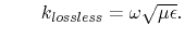 |
(4.6) |
A formulation for the voltage U on the planes is obtained by
multiplying (4.6) with the plane separation distance h:
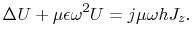 |
(4.7) |
Equation (4.6) is expressed as a two-dimension transmission line
equation
 |
(4.8) |
with
 and and |
(4.9) |
According to transmission line theory, the introduction of conduction and dielectric
losses into (4.8) yields
![$\displaystyle \Delta U+[\omega^{2} L_{c}'C_{c}'-j(C_{c}'R_{c}'+L_{c}'G_{c}')-R_{c}'G_{c}']U=(j\omega
L_{c}'+R_{c}')J_{z}.$](img247.png) |
(4.10) |
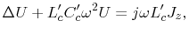
The surface resistance which considers conduction losses is
Where  and
and  are the surface resistances of the lower and upper
plane respectively. With i=1 and i=2 for the two planes,
are the surface resistances of the lower and upper
plane respectively. With i=1 and i=2 for the two planes,  is the plane
thickness,
is the plane
thickness,
 is the conductivity of the plane metal, and
  is the
skin depth of the plane.
The dielectric losses of the isolation layer are considered
in (4.10) by
is the
skin depth of the plane.
The dielectric losses of the isolation layer are considered
in (4.10) by
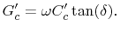 |
(4.12) |
Where
 is the loss tangent of the material. To meet the
requirement (4.4), the term
is the loss tangent of the material. To meet the
requirement (4.4), the term
 of (4.10) must be small compared to
 . On the right
hand side term
. On the right
hand side term
 ,
,  must be small compared to
 . This is in fact the case for the indented application of the method, because of
the highly conducting metallic planes and the significant portion of air in the volume.
Therefore, these terms can be neglected. With this simplification (4.9)
and (4.12), the equation for the voltage distribution inside the cavity,
becomes
. This is in fact the case for the indented application of the method, because of
the highly conducting metallic planes and the significant portion of air in the volume.
Therefore, these terms can be neglected. With this simplification (4.9)
and (4.12), the equation for the voltage distribution inside the cavity,
becomes
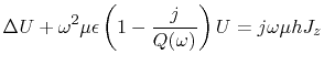 with with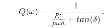 |
(4.13) |
 is the total quality factor which considers the conduction and the dielectric
losses.
is the total quality factor which considers the conduction and the dielectric
losses.
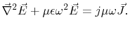
Finally, the Helmholtz equation for the electric field strength, which considers
conduction and dielectric losses is
 |
(4.14) |
Subsections
C. Poschalko: The Simulation of Emission from Printed Circuit Boards under a Metallic Cover
 with
with