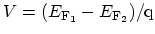
For ballistic transport one can consider an ideal case where electrons are not
scattered on the wire of length  connected to two electrodes,
  and
and  (see Fig. 2.13). Since two electrodes have a large electron
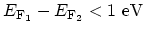
capacity, the FERMI energy for electrodes and are
constants denoted by
(see Fig. 2.13). Since two electrodes have a large electron
capacity, the FERMI energy for electrodes and are
constants denoted by
 and
and
 ,
(
,
(
 ), respectively. If
there are no reflections of electrons at the electrodes,
), respectively. If
there are no reflections of electrons at the electrodes,  states are
occupied primarily by electrons coming from the left contact while the
states are
occupied primarily by electrons coming from the left contact while the  states are occupied primarily by electrons coming from the right
contact. Consequently the occupation factors for the and states are
given by the FERMI functions for the left and right contacts, respectively.
states are occupied primarily by electrons coming from the right
contact. Consequently the occupation factors for the and states are
given by the FERMI functions for the left and right contacts, respectively.
Figure 2.13:
A ballistic conductor with length is
connected to two electrodes and with FERMI energies
and
, respectively.
 is the number of channels for
electrons to propagate from the electrode to .
is the number of channels for
electrons to propagate from the electrode to .
|
|
Because of the confinement of electronic states in the direction perpendicular
to the current flow, there are several energy subbands
 .
Thus the total current is given by the sum of the
microscopic currents of all the subbands
. The subbands
are also called channels. The number of channels is a function of energy, which
is denoted by
.
Thus the total current is given by the sum of the
microscopic currents of all the subbands
. The subbands
are also called channels. The number of channels is a function of energy, which
is denoted by  . An electron which has a velocity of
 in an unoccupied state contributes
to the microscopic current
in an unoccupied state contributes
to the microscopic current
 , in which
 is the
carrier transit time
is the
carrier transit time
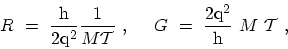
 . Then the total current is
given by [60]
. Then the total current is
given by [60]
![\begin{displaymath}\begin{array}{ll} I \ & \displaystyle = \ \frac{\ensuremath {...
...\mathrm{F}_2}\right]}{\ensuremath {\mathrm{q}}} \ , \end{array}\end{displaymath}](img364.png) |
(2.21) |
where the sum over  is converted to the integral. In (2.21) a spin
degeneracy of and the inverse of the level spacing
is converted to the integral. In (2.21) a spin
degeneracy of and the inverse of the level spacing  is introduced and
is assumed to be constant over the integration range. One can easily
show that for
is introduced and
is assumed to be constant over the integration range. One can easily
show that for
 only states with
 contribute to the total current. If the width of a wire is very small
(less than
contribute to the total current. If the width of a wire is very small
(less than
 ),
),  even for
 .
On the other hand, if the width of a wire is on the order of
.
On the other hand, if the width of a wire is on the order of
 and
, the number of channels
becomes very large (
and
, the number of channels
becomes very large ( ).
).
Since
 is the voltage between the
electrodes, the resistance of the ballistic conductor is given by
is the voltage between the
electrodes, the resistance of the ballistic conductor is given by
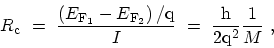 |
(2.22) |
where
 is called the contact resistance and
 is the
quantized resistance
is the
quantized resistance
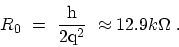 |
(2.23) |
This contact resistance arises from the mismatch of the numbers of conduction
channels in the mesoscopic conductor and the macroscopic metal
lead [60]. In addition to this quantum-mechanical contact
resistance, there are other sources of contact resistance, such as that
produced by poor coupling between the mesoscopic conductor and the leads. The
inverse of (2.22) gives the contact conductance
 where
where
 denotes the quantized conductance.
Thus in a wire without scattering the conductance is
proportional to . The quantized resistance and conductance can be observed
in clean semiconductors at very low temperature on samples which have a small
number of channels [61]. If one considers the range of
for a SW-CNT with a diameter of
denotes the quantized conductance.
Thus in a wire without scattering the conductance is
proportional to . The quantized resistance and conductance can be observed
in clean semiconductors at very low temperature on samples which have a small
number of channels [61]. If one considers the range of
for a SW-CNT with a diameter of
 , one finds that
under low bias conditions,
, one finds that
under low bias conditions,
 .
In a zigzag SW-CNT close to the FERMI energy the bands are doubly
degenerate, and thus the total conductance is
.
In a zigzag SW-CNT close to the FERMI energy the bands are doubly
degenerate, and thus the total conductance is  .
.
In case of coherent transport, the wave-function
is determined by the SCHRÖDINGER equation. The phase
and amplitude of the wave-function at electrode can be obtained from those
at electrode . The resistance and the conductance are thus given by
 |
(2.24) |
where
 is the transmission probability for a channel extending from
electrode to electrode . Here it is assumed again that
is
constant near the FERMI energy. Equation (2.24) is known as the
LANDAUER formula. It can be applied only if the wave-function
spreads over the whole sample.
is the transmission probability for a channel extending from
electrode to electrode . Here it is assumed again that
is
constant near the FERMI energy. Equation (2.24) is known as the
LANDAUER formula. It can be applied only if the wave-function
spreads over the whole sample.
The resistance
 for a single channel of a mesoscopic wire is
given in terms of the transmission probability
as
for a single channel of a mesoscopic wire is
given in terms of the transmission probability
as
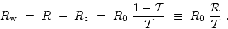 |
(2.25) |
The reflected wave-function, which is proportional to
 , causes a voltage drop in the wire.
M. Pourfath: Numerical Study of Quantum Transport in Carbon Nanotube-Based Transistors
![\includegraphics[width=.47\textwidth]{figures/Conduct_Quant.eps}](img357.png)