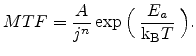
Electromigration is the transport of material caused by the gradual movement of the atoms in a conductor due to the momentum transfer between conducting electrons and diffusing metal atoms. All work in this field was pioneered by James R. Black [85], who established the basis. Accordingly, Black's semi-empirical equation, developed at the end of 1960s, is given by:
 |
(5.1) |
It describes the median time to failure (MTF) caused by electromigration, where
![]() is a pre-exponential constant based on the cross-sectional area of the
interconnect,
is a pre-exponential constant based on the cross-sectional area of the
interconnect, ![]() is the activation energy,
is the activation energy,
![]() is Boltzmann's constant,
is Boltzmann's constant, ![]() is the temperature,
is the temperature,
![]() is the current density, and
is the current density, and ![]() is the so-called current density exponent.
The problem with this formula is, that the activation energy
is the so-called current density exponent.
The problem with this formula is, that the activation energy ![]() and the
current density exponent
and the
current density exponent ![]() have to be determined experimentally and therefore
its validity is limited to specific test configurations. In order to understand
the phenomenon of electromigration, a more physical approach based on the
main diffusion scenes within interconnect structures must be applied.
have to be determined experimentally and therefore
its validity is limited to specific test configurations. In order to understand
the phenomenon of electromigration, a more physical approach based on the
main diffusion scenes within interconnect structures must be applied.
 |
The mechanism of electromigration can be explained by the interaction of two counteracting forces:
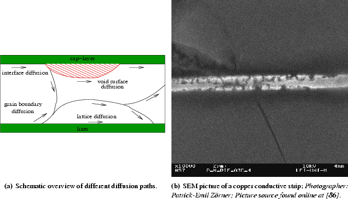
A schematic overview of different diffusion paths is shown in
Figure 5.1(a). Local mass flux divergences cause the formation, growth,
and movement of voids and hillocks. Especially the movement of electromigration
induced voids is very
challenging to model, since the simulation domain and, therefore, also the spatial
discretization changes its structure after every time step. Voids can grow and
shrink, they can move within Cu lines, aggregate, and split. These changes have
to be considered during a time dependent electromigration simulation where
primarily the interface between a void and the surrounding environment has to
be tracked carefully.
The following is mostly focused on modeling the movement of voids within an arbitrary interconnect structure and the development of a powerful mesh adaptation technique which allows to use a diffuse interface model for the description of the metal void interface.