
 |
|
Biography
Hajdin Ceric was born in Sarajevo, Bosnia and Herzegovina, in 1970. He studied electrical engineering at the Electrotechnical Faculty of the University of Sarajevo and the Technische Universität Wien, where he received the degree of Diplomingenieur in 2000. In 2005 he received his PhD in technical sciences and in 2015 his venia docendi in microelectronics from the Technische Universität Wien. In 2010 he was appointed the head of the Christian Doppler Laboratory for Reliability Issues in Microelectronics. He is currently an Associate Professor at the Institute for Microelectronics. His research interests include modeling and simulation of reliability issues in interconnects for ultra large-scale integration.
The Impact of Scaling on Nano-Interconnect Reliability
The drastic reduction of nano-interconnect linewidth - towards 10 nm and below - has had a tremendous impact on the nature of electromigration failure. Mitigation of electromigration degradation for such down-scaled interconnects will require an in-depth understanding of the relevant failure mechanisms and the development of adequate simulation models on the basis of this understanding. Numerous previous studies have shown that there is a relationship between electromigration failure and the microstructure of Cu. Describing and including this relationship in models used for electromigration simulation is of crucial importance to the continued engineering of reliable interconnects. Interconnect scaling has led to significant changes in the microstructure of the Cu line, where poly-crystalline sections increasingly dominate large portions of the interconnect's length.
Modeling of electromigration in each single grain and at the grain boundaries is possible, but it would be a time-consuming venture, particularly if, for the sake of accuracy, we need to include in the simulation as large a portion of the interconnects' layout as possible. To reconcile these demands we choose to describe interconnect portions with finer grains by utilizing only effective values, while simulating the grain boundaries of larger grains using a more detailed model.
The crucial parameter required for an estimation of many key quantities - such as effective values for diffusivities, effective valences and recombination times for interconnect metal containing a network of grain boundaries embedded in different types of interface layers - is the volume fraction of grain boundaries in the metal body. This parameter can be estimated using Smith's theory, from SEM/TEM pictures or by means of microstructural simulation (e.g. the Monte Carlo Potts model). Modeling of void dynamics, which include void growth and migration, is an important part of interconnect lifetime-prediction modeling. Intrinsic voids in metal lines are responsible for resistance growth and final failure. The normal velocity of the void surface is composed of four components: The elastic strain energy velocity component, the electromigration velocity component, the surface free energy velocity component, and the vacancy absorption velocity component. For a basic lifetime estimate, it is sufficient to assume that a void maintains during its growth some simple geometrical shape - such as a cylinder or ellipsoid - and that for an actual void growth velocity, a maximum normal velocity calculated at the void surface is taken. This represents the worst-case scenario for lifetime prediction.
In Fig. 1a, an example of an interconnect line with via is presented. The microstructure is modeled either as a full grain or as an effective grain domain that includes poly-crystalline sections of the interconnect. In the presented case, the blue domain represents a full grain domain and the green one a poly-crystalline domain. The ellipsoid void under study straddles both of these domains, which are for the purposes of accurate simulation meshed with a finer FEM mesh. An important accompanying effect of void growth is a current flow necking that leads to an increase in void surface velocity (see Fig. 2b). Detailed modeling of void growth allows for a thorough study of the effect of interconnect narrowing on its lifetime. In Fig. 3, the dependence of the void surface velocity on the void radius for different interconnect thicknesses is displayed. The most important result provided by such a study is the prediction of resistance increase due to void growth (see Fig. 3). By combining the simulation results presented in Figs. 2 and 3, an estimation of interconnect lifetime is carried out.
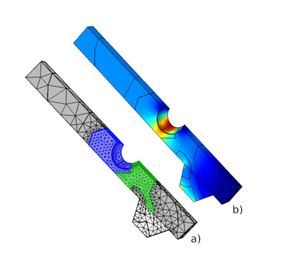
Fig. 1: Ellipsoid void growing into an interconnect line. a) Finer meshes for single grain domain (blue) and poly-crystalline domain (green). b) During void growth, peak current density develops on the top of the void.
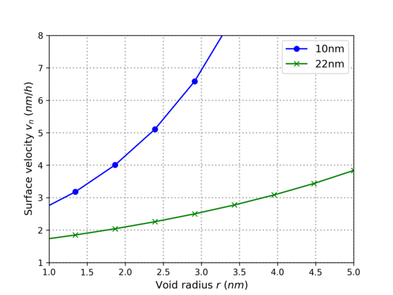
Fig. 2: Normal velocity of the void surface for interconnect thicknesses of 10 nm and 22 nm.
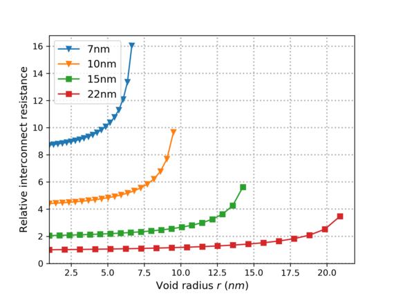
Fig. 3: Increase of interconnect resistance with void growth for interconnect thicknesses of 7 nm, 10 nm, 15 nm, and 22 nm.