 |
|
Biography
Lado Filipovic studied electrical engineering at Carleton University, in Ottawa, Canada, where he received the degree of Bachelor in electrical engineering (B.Eng.) in 2006 and Master in applied science (M.A.Sc) in 2009. He joined the Institute for Microelectronics in January 2010, where he completed his doctoral degree in December 2012, which focused on topography simulations of novel semiconductor processes. Since then his scientific interest have broadened to studying and modeling the effects of fabrication-induced variability on semiconductor geometries and their application in the fabrication of quantum metrology devices. His added research interests involve the design and simulation of environmental sensors and, more specifically, using metal oxide semiconductors for the detection of toxic gases and pollutants.
Including Grain Boundaries and Material Interfaces
in Electromigration Simulations
The continuing trend in transistor scaling over the last decades according to Moore's Law must be supported by a simultaneous scaling of the interconnect lines. Currently, many alternate materials and structures are being investigated to replace copper and further shrink transistor dimensions, which is starting to become a bottleneck in circuit scaling and performance. Mitigating the impact of size effects, including surface roughness and the increased presence of grain boundaries, is essential if scaling is to continue. The most commonly used metal, copper (Cu), is starting to show undesirable behavior at the nanoscale, including increasing resistivity and electromigration (EM) effects as the interconnect shrinks. While these effects result in undesirable performance, it is still expected that copper will continue to be used in devices for the next several technology nodes and will remain the preferred solution for interconnect metals until at least 2021.
Due to the increased influence of the microstructure on the operation and lifetime of copper interconnects, it is essential to include grain boundaries and material interfaces in technology computer-aided design (TCAD) lifetime simulations. Currently, the influence of the microstructure is included in EM simulations by using an effective diffusivity parameter (Deff), which is a combination of the bulk (DB) and grain boundary (DGB) diffusivities, and using this value in continuum or bulk simulations with
Deff = DB + DGB/D * tGB,
where D is the mean grain size and tGB is the effective grain boundary thickness. The alternative is to explicitly describe the grain boundaries and material parameters as independent materials and to mesh the full structure. This method results in very complex and fine meshes, however, reducing the simulation space to only a few grains. We have developed an alternative framework, where we can model a full interconnect line, while treating the grain boundaries and material interfaces using spatial parameters, which are read in by the finite element electromigration TCAD simulator. The proposed flow provides for the interconnection of a variety of tools, including a tessellation software and EM simulator. The three steps are pictured in Fig. 1 and can be described as follows:
- Grain tessellation: The open-source tool Neper is used to generate a crystalline geometry using Vonoroi tessellation.
- Spatial parameter assignment: The microstructure from Neper is imported into an in-house tool, where a Cartesian grid is generated. Each point on the grid is assigned several parameter values, including distance to the nearest boundary and atom diffusivity.
- Electromigration simulation: Finally, the spatial parameters are imported into a finite element simulator and the EM model is implemented. The electro-thermo-mechanical problem is then initiated with an applied electric field and ambient temperature to replicate accelerated failure conditions.
This framework allowed us to simulate the vacancy and stress build-up in an interconnect line with almost 100 grains within minutes. We also note the ability of the framework to properly treat triple points, where a grain boundary and material interface meet, even when a very coarse Cartesian mesh is applied. In Fig. 2, the stress build-up at a triple point is plotted with time while the mesh is varied, showing a 5% variation, even when the grid is increased from 0.4 nm to 2 nm. This resulted in a reduction in the simulation time from 160 minutes to 10 minutes for grid resolutions of 0.4 nm and 2 nm, respectively, as shown in Fig. 3.

Fig. 1: Three phases of the implemented modeling framework to properly simulate EM in copper nano-interconnects, while taking grain boundaries and material interfaces into consideration.
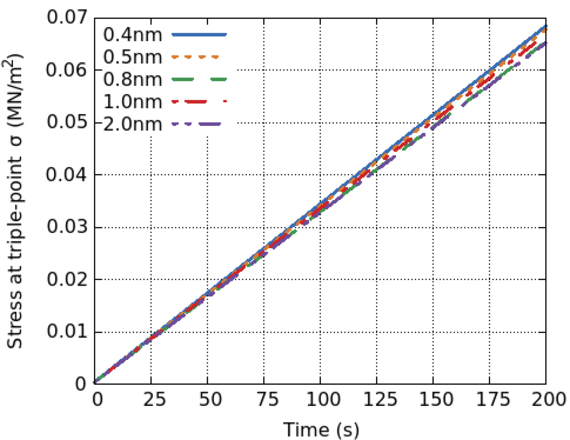
Fig. 2: EM-induced hydrostatic stress (NM/m2) at a triple point when using different mesh resolutions with the grain boundary thickness set to 1 nm.
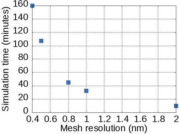
Fig. 3: The dependence of the mesh resolution on the simulation time for the EM simulation given in Fig. 2.