 |
|
Biography
Alexander Makarov was born in Volgograd, Russia, in 1985. He studied information technology at the Volgograd State Technical University, where he received the BSc degree in 2006 and MSc degree in 2008. He joined the Institute for Microelectronics in October 2009 and has obtained the doctoral degree in March 2014. He is currently employed as a post-doc researcher. His scientific interests include Monte-Carlo simulations and nonvolatile memory device modeling.
Modeling the Effect of Random Dopants on Hot-Carrier Degradation in FinFETs
Hot-carrier degradation (HCD) is recognized as one of the most important phenomena amongst degradation modes. With the rapid shrinking of device dimensions, the detrimental effect of HCD becomes more pronounced, and recently, HCD was reported as the main reliability issue in most advanced FinFET nodes fabricated by Intel. The situation becomes even more complicated since ultra-scaled transistors contain just a handful of randomly located dopants. As a result, these devices can have wide spreads in their parameters, such as the drain current, threshold voltage, etc. A related problem is that changes in these parameters during hot-carrier (HC) stress, as well as Bias Temperature Instability (BTI), time-dependent dielectric breakdown (TDDB), etc., cannot be described using a single degradation trace resulting in a single device lifetime value.
Instead, comprehensive modeling of any of the reliability phenomena in nanoscale FETs should include a statistical analysis. Such a statistical analysis has already been applied to the intimately related degradation issues BTI, random telegraph noise and TDDB. As for HCD, extensive experimental efforts focused on the statistical description of this effect have been performed. Moreover, some modeling approaches that study the impact of random positions of interface traps generated during HC stress have recently been published. These approaches do not capture the effect of random dopants on HCD, however, and for this, simulations must be performed for a device with a fixed configuration.
To achieve this, we used an ensemble of 200 FinFETs with different configurations of random dopants and calculated carrier energy distribution functions, interface state density profiles, linear drain current degradation traces and lifetimes for each of these devices, as well as for a device with an average doping profile (Fig. 1). We found that in all cases HCD (and related quantities) is overestimated if treated with the deterministic version of the model. In addition, device lifetimes have rather broad distributions. For higher stress voltages, their probability densities are nearly normally distributed, while for a regime similar to operating conditions, the lifetime distribution substantially deviates from the Gaussian. Therefore, full statistical treatment should be carried out to describe HCD in sufficient detail.
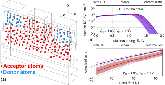
Fig. 1: (a) A schematic representation of the FinFET with random dopants. (b) Families of electron energy distribution functions calculated for Vds = 1.8 V and Vgs = 1.9 V plotted in the drain sections in the device. In addition, the distribution functions for the nominal device and the average distribution functions are shown. (с) Families of ΔId,lin(t) changes obtained for Vds = 1.8 V and Vgs = 1.9 V. Deterministic and average ΔId,lin(t) traces are also plotted.