3.2 Small Signal Equivalent Circuit
Parameter Extraction
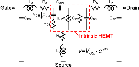
The HEMT can be described by an equivalent circuit model shown in
Figure
3.1. To extract the model parameters from measured Sparameters
a value for each parameter of the model is assumed and Sparameters
are calculated based on the equivalent circuit. The chosen values are then
optimized by minimizing the differences between the calculated and the
measured Sparameters.
The transit frequencies fT and fmax
can be traced back to equivalent circuit parameters. From the intrinsic
device the well known approximation for the current gain cut-off frequency
fT can be derived as
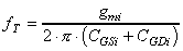 . . |
(10)
|
According to [37,
38]
fmax can also be approximated with equivalent circuit
parameters by:
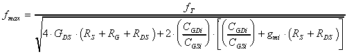 . . |
(11)
|
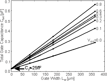
Based on the equivalent circuit the parameters can be extracted from measured Sparameters. In the extraction procedure it is difficult to distinguish between the parasitic pad capacitances CPG and CPD and the gate source capacitance CGS because they are connected in parallel and therefore only their sum can be determined reliably. In first order CPG and CPD are the only capacitances which do not scale with the gate width Lw. This can be used to extract these values in a different way.
The measured value of fT includes all capacitances.
The total capacitance can be determined rearranging (10)
to
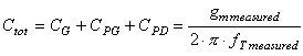 . . |
(12)
|
The schematic of the extrinsic device used for simulation is shown in
Figure
2.1 It corresponds to the intrinsic device indicated by the dashed
box in Figure
3.1 and the parasitic resistances RS, RG,
and RD. The deembedded device parameters will be the
basis for comparison between measured and simulated data.
![]()
![]()
![]()
![]()
Next: 3.3 Determination of Capacitances
by Quasi Static Approximation Up: 3 Measurement
and Parameter Extraction Previous: 3.1
DC and RF Measurements
Helmut Brech 1998-03-11