


Next: 6.2 Development of an
Up: 6. Applications of the
Previous: 6. Applications of the
The basic structure of a FinFET published in [9] is shown in Figure 6.1. The silicon layer is formed as silicon on insulator (SOI). The fin is formed as a small silicon finger. For a better carrier absorption the source and drain regions are realized as large silicon pads. The active device area is the small fin region under the polysilicon gate. To obtain higher drive currents, additional fins can be applied in parallel.
As the polysilicon is separated from the silicon by a thin oxide layer, the current density inside the silicon fin can be controlled by the gate voltage.
Figure 6.1:
Geometry of the simulated FinFET structure.
|
|
Depending on the device design we can distinguish between different kinds of FinFETs. Every side of the fin surrounded by the gate can be used as a control contact.
If the surrounding oxide is thin, the charge carriers are controlled by the gate voltage. Using a thick oxide, the gate voltage does not influence the carriers. Generally there are two possibilities:
- In double gate FinFET only two sides of the fin are enclosed by a thin oxide. The upper face has a thick oxide. Here the carriers on both sides of the fin can be controlled. This device is usually simulated by a two-dimensional simulation. However, effects at the corners of the fin can there not be accounted for. Actually at these regions the electric field is much higher and a higher current density will be obtained. These effects can only taken into account by three-dimensional simulations.
- In triple gate FinFET all three sides of the fin are enclosed by a thin oxide. Therefore, the carriers on all three sides can be controlled. In this case, the upper plane cannot be described by two-dimensional geometries and the device simulation has to be performed three-dimensional.
In Figure 6.2 an ortho grid is used for the simulation. Therefore, every grid line continues through the whole device. The active area is only the small part of the fin surrounded by the polysilicon. There the grid density must be high. As a negative sideffect, the high grid line density propagates through all other segments. A unnecessarily high grid line density is produced in these other segments and the global amount of grid points is too high. Especially in the insulator segments, the grid density could be much cruder. Fragments of this grid line propagation can be seen as dense clustered grid lines on the surface of the oxide layer, which are caused by the dense grid lines in the fin.
Figure 6.2:
The oxide and silicon layers of the FinFET structure. The simulation grid is an ortho grid. The grid elements are split to tetrahedrons only for visualization purposes.
|
|
Figure 6.3:
The oxide and silicon layers of the FinFET. The simulation grid is generated by the potential method. In the source and drain regions the approximation of the grid lines to the current lines can be seen.
|
|
Figure 6.4:
Generated ortho grid in the active regions of the transistor. Only the oxide, silicon and polysilicon segments are shown.
|
|
Figure 6.5:
Potential based tetrahedral grid in the active regions of the transistor. Only the oxide, silicon and polysilicon segments are shown.
|
|
The grid resulting from the potential method is shown in Figure 6.3. The grid density can be controlled for each segment and the amount of grid points is much smaller.
A detail of the structure is shown in the next figures. Here only the silicon layer is drawn. Figure 6.4 shows the ortho grid, Figure 6.5 the potential based grid. The silicon segment can be split into three different regions:
- The active area in the middle of the fin. The grid density must be high in all three directions of space. The carrier concentration and current density distribution must be properly resolved in all three directions.
- The outer fin areas, which are attached on the left and right sides of the active area.
The current density does not change much along the fin. The grid density along the fin can be cruder. No radial imposed electric field is present and the differences in the current density settle down, therefore, across the fin the current must be pretty good resolved.
- In the source and drain region the current lines spread out.
Miscellaneous current density differences are settled and a crude grid can be chosen. The current lines inside the fin spread out in the regions of the contacts.
In terms of the current flow, the grid lines are a good approximation of the current flow.
The different approaches are compared in Table 6.1. They were performed by the device simulator MINIMOS-NT [11] on an IBM p-Series machine with 1400 MHz Power 4+ processors.
A third simulation was performed on a potential based grid, which is refined in the the active areas of the fin. The according output characteristics of the potential based simulations are shown in Figure 6.1. No significant change of the characteristic is determined by the different grids. The high ratio of grid elements to grid points of the potential method based grids compared to the ortho grid is caused by the different type of grid elements.
Contour lines of the current density in the active fin area are shown in Figure 6.1.
Table 6.1:
Comparison of the different grids. Rank describes the rank of the system matrix of the equation system assembled by MINIMOS-NT, which was used for the electrical simulation.
| Grid type |
Points |
Elements |
Elem. type |
Rank |
Sim. time |
| Ortho grid |
48,480 |
42,840 |
Cuboids |
83,998 |
124m30s |
| Potential method 1 |
11,186 |
32,666 |
Tetrahedrons |
16,238 |
38m39s |
| Potential method 2 |
42,404 |
128,819 |
Tetrahedrons |
65,132 |
390m10s |
|
Figure 6.6:
Simulated output characteristic of the FinFET. The drain current
 is standardized by the gate length
 .
.
|
|
Contour lines of the electron current density in the chanel area of the fin at
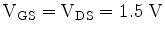
.
Next: 6.2 Development of an
Up: 6. Applications of the
Previous: 6. Applications of the
J. Cervenka: Three-Dimensional Mesh Generation for Device and Process Simulation
![\includegraphics[width=8.8cm]{picsconveps/finortho}](img651.png)
![\includegraphics[width=8.8cm]{picsconveps/fintet}](img652.png)
![\includegraphics[width=9.2cm]{picsconveps/det}](img653.png)
![\includegraphics[width=9.2cm]{picsconveps/detail}](img654.png)
![\includegraphics[width=12.5cm]{htmlpicsconveps/newcrv3}](img655.png)
![\includegraphics[width=12cm]{picsconveps/xxx}](img649.png)
![\includegraphics[width=2.5cm]{picsconveps/materialfin}](img650.png)
![\includegraphics[width=11cm]{picsconveps/hhh}](img657.png)