In the next example, the interaction of the different tools for the development of an EEPROM memory cell will be demonstrated.
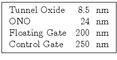
The goal was to extract characteristic values of an EEPROM memory cell. For timing analysis, the capacitances between the semiconductor segment and the control- and floating-gate are crucial. To allow the extraction of these capacitances the three-dimensional extraction of the electric field is necessary. As it is impossible to describe such a complex device structure manually, the device structure had to be generated by a fully three-dimensional simulation of all the manufacturing processes of the device. The cross section of the memory cell and its typical layer thicknesses are shown in Figure 6.8.
While initial process steps like the oxidation of the silicon wafer for generating the field-oxide can be performed by a two-dimensional analysis, the following process steps have to be performed fully three-dimensional:
The final electrical simulation and capacitance extraction is performed with the simulator STAP, part of the Smart Analysis Programs [55][56]. This is a three-dimensional interconnect simulator, which computes the field distribution inside the simulation area using Finite Elements. The capacitances are calculated via the energy of the electric field [54]. The result of the field calculation can be seen in Figure 6.13. An explanation for the large number of grid points and tetrahedrons is a global grid refinement of the program STAP, where each tetrahedron is split into 8 smaller ones. The floating-gate and the control-gate segments are connected to constant potential, 0 V and 1 V, respectively. The influence of the silicon segment is taken into account as a ground plane (connected to 0 V). Within this figure, the contact regions, which are the floating-gate, the control-gate, and the silicon segment, have been removed. Results of the capacitance extraction are shown in Table 6.2.
![\includegraphics[width=10cm]{ex3pics/pot.eps}](img666.png)
![\includegraphics[width=2cm]{ex3pics/bar.eps}](img667.png)
|
It is remarkable that the basically simple silicon/oxide-structure,
starting with 51,000 tetrahedrons, increases to 400,000 tetrahedrons and
the memory limits during process simulation are reached.
However, the
field extraction is performed by 3,400,000 tetrahedrons
and the memory consumption is not of this magnitude.
The enormous process simulation overhead in memory consumption is caused by the required functionality of the process simulation tools. In detail, for deposition and etching at least two grids, the original and the modified grid, are stored during each simulation step. Additional functionality, such as neighborhood information, surface information, an octree for point location and additional attributes have to be stored in the data structures. For performing the interconnect simulation, only the final grid and potential attributes are necessary.
For future simulations of more complex three-dimensional structures
further work on data reduction and surface smoothing will be
necessary.
|
![$\textstyle \parbox{8cm}{\includegraphics[width=\linewidth]{picsconveps/zelle2}}$](img658.png)
![\includegraphics[width=10.5cm]{picsconveps/structure}](img660.png)
![\includegraphics[width=2.5cm]{picsconveps/materialee}](img661.png)
![\includegraphics[width=10.5cm]{picsconveps/ono1}](img662.png)
![\includegraphics[width=10.5cm]{picsconveps/ono31}](img663.png)
![\includegraphics[width=10.5cm]{picsconveps/poly21}](img664.png)