


Next: 4.2 DCIV Method
Up: 4. Characterization of Interfaces
Previous: 4. Characterization of Interfaces
Subsections
4.1 Charge Pumping Method
The charge pumping method has shown to be a very reliable and also precise
method allowing the in-depth analysis of the interface, directly in the MOSFET
device. Additionally it only requires basic equipment and is relatively easy
to set up.
The effect has been first reported by Brugler and Jespers in
1969 [39]. They reported a net DC substrate current when applying
periodic pulses to the gate of a MOS transistor, while keeping source and drain
grounded. The current was found to be proportional to the gate area and the
frequency of the applied gate pulses. It was flowing in the opposite direction
of the leakage current of the source and drain to substrate diodes. They
showed that the current originates from recombination of minority and majority
carriers at traps at the
 interface. Therefore, the method can be used
for measuring the interface trap density in MOSFETs for the evaluation of
MOSFET degradation. The major breakthrough for the charge pumping method was
the thorough investigation and correct explanation of the method, applied
directly to MOSFET structures by Groeseneken et al. in
1984 [40].
interface. Therefore, the method can be used
for measuring the interface trap density in MOSFETs for the evaluation of
MOSFET degradation. The major breakthrough for the charge pumping method was
the thorough investigation and correct explanation of the method, applied
directly to MOSFET structures by Groeseneken et al. in
1984 [40].
Figure 4.1:
Basic experimental setup for the charge pumping measurement. The
source to substrate and drain to substrate diodes are typically slightly
reverse biased while the gate is pulsed between inversion and accumulation
conditions. The substrate current is measured as the charge pumping current
 .
.
|
|
The basic experimental setup for the charge pumping method can be seen in
Figure 4.1 for an n-channel MOSFET. The source and drain to
substrate diodes are reverse biased. The gate is pulsed between accumulation
and inversion conditions while the charge pumping current is measured at the
substrate. This current flows in the opposite direction of the source and
drain to substrate diode leakage currents.
Figure 4.2:
Base level sweep during a charge pumping measurement. As the base
and also the top level of the gate pulse pass the flat-band and threshold
voltage levels of the transistor, five different regimes can be
distinguished.
|
|
In the accumulation phase majority carriers, holes in case of an n-channel
MOSFET, flood the channel area and some of them become trapped in interface
traps. When the gate pulse drives the transistor into inversion, the majority
carriers leave the channel and move back to the substrate. Some trapped
carriers with energies close to the valence band can be de-trapped through
thermal emission before the channel becomes flooded by electrons and also move
back to the substrate. The rest of the trapped holes recombines with channel
electrons and leads to a net current. The same process occurs when the
transistor is driven from inversion back to accumulation, with opposite carrier
types.
The base level of the gate voltage pulse is swept to drive the MOSFET from
accumulation to inversion. When the amplitude of the pulse is larger than the
difference of threshold voltage and flat-band voltage,
 , then five different regimes are observed as sketched in
Figure 4.2. Regime 3, where the largest amount of traps in the
band-gap is scanned, is the most important one. It can be described by a
current model (Section 4.1.2) to calculate the interface trap
density. The base level sweep charge pumping method was first proposed by
Elliot [41] and the different regimes are governed by the following
mechanisms:
, then five different regimes are observed as sketched in
Figure 4.2. Regime 3, where the largest amount of traps in the
band-gap is scanned, is the most important one. It can be described by a
current model (Section 4.1.2) to calculate the interface trap
density. The base level sweep charge pumping method was first proposed by
Elliot [41] and the different regimes are governed by the following
mechanisms:
The whole pulse is below the flat-band voltage and the
substrate is in permanent accumulation. The interface traps are permanently
filled with holes and therefore no recombination current is measured.
The top of the pulse reaches the region between the
flat-band and the threshold voltages. In this phase the interface is moved
from accumulation into strong depletion up to weak inversion. Here, the
charge pumping current increases and the base voltage is around threshold
voltage minus the pulse height. It could be assumed that the shape of the
rising
 in this regime is determined by the recombination process in
weak inversion. It has been shown, though, that other mechanisms may have an
important influence. These can be surface potential fluctuations because of
spatially non-uniformly distributed oxide
charges [42,43], acceptor and donor
traps [43], or variations in the proximity of the source and
drain regions. Also the modulation of the effective gate area by the gate
voltage might influence the rising charge pumping current.
The base level voltage is below the flat-band voltage,
and the top level of the pulse is above the threshold voltage,
in this regime is determined by the recombination process in
weak inversion. It has been shown, though, that other mechanisms may have an
important influence. These can be surface potential fluctuations because of
spatially non-uniformly distributed oxide
charges [42,43], acceptor and donor
traps [43], or variations in the proximity of the source and
drain regions. Also the modulation of the effective gate area by the gate
voltage might influence the rising charge pumping current.
The base level voltage is below the flat-band voltage,
and the top level of the pulse is above the threshold voltage,
 . In this regime the charge pumping pulse sweeps the
substrate in the channel area from accumulation to complete inversion. At
each time the transistor is pulsed from accumulation to inversion or back.
The fast interface traps are filled with holes, or electrons, respectively,
which then recombine with the opposite carrier type leading to a net current
measurable as
. In this regime the current has the highest magnitude.
The base level is between the flat-band and threshold
voltages. The transistor only reaches weak accumulation, the interface traps
are mainly negatively charged and are no longer flooded with holes, thus
recombination is reduced and the charge pumping current goes down. The same
surface potential fluctuation and gate area modulation effects as in Regime 2
can influence the characteristic of
.
The transistor is completely in inversion during the
whole pulse. The traps are filled with electrons and no holes reach the
channel at any time. The measured substrate current only consists of the
source and drain leakage currents.
. In this regime the charge pumping pulse sweeps the
substrate in the channel area from accumulation to complete inversion. At
each time the transistor is pulsed from accumulation to inversion or back.
The fast interface traps are filled with holes, or electrons, respectively,
which then recombine with the opposite carrier type leading to a net current
measurable as
. In this regime the current has the highest magnitude.
The base level is between the flat-band and threshold
voltages. The transistor only reaches weak accumulation, the interface traps
are mainly negatively charged and are no longer flooded with holes, thus
recombination is reduced and the charge pumping current goes down. The same
surface potential fluctuation and gate area modulation effects as in Regime 2
can influence the characteristic of
.
The transistor is completely in inversion during the
whole pulse. The traps are filled with electrons and no holes reach the
channel at any time. The measured substrate current only consists of the
source and drain leakage currents.
4.1.2 Charge Pumping Current Model
Figure 4.3:
Charge pumping signal applied to the gate contact. The signal is
characterized by the rise and fall times,
 and
and
 , and the amplitude
 . For the emission of
electrons and holes from the traps only the window between the flat-band
voltage
. For the emission of
electrons and holes from the traps only the window between the flat-band
voltage
 and the threshold voltage
 is significant.
|
|
The first comprehensive model for the charge pumping current was proposed by
Groeseneken et al. in 1984 [40]. This model has been
developed to capture the maximum charge pumping current which is obtained in
Regime 3. Here the gate voltage pulse sweeps from below the flat-band voltage
to above the threshold voltage. Therefore the substrate is driven from
accumulation to inversion and back.
Only the fast interface traps situated between the two energy levels
 and
and
 in the band-gap of the semiconductor
can contribute to the charge pumping current,
in the band-gap of the semiconductor
can contribute to the charge pumping current,
 |
(4.1) |
 |
(4.2) |
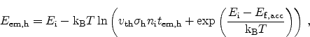
where  is the intrinsic energy,
 and
and
 are the Fermi energies in inversion and accumulation,
 is the thermal velocity,
 the capture
cross sections of the traps, and
the capture
cross sections of the traps, and  is the intrinsic carrier
concentration. Traps outside this band cannot contribute to the current as the
trapped charge becomes de-trapped instantly through thermal emission when the
Fermi-level moves beyond the trap level, for trapped electrons, or above, for
trapped holes.
is the intrinsic carrier
concentration. Traps outside this band cannot contribute to the current as the
trapped charge becomes de-trapped instantly through thermal emission when the
Fermi-level moves beyond the trap level, for trapped electrons, or above, for
trapped holes.
The emission times
 and
and
 for electrons and
holes can be calculated from the fall and rise times,
for electrons and
holes can be calculated from the fall and rise times,  and
and
 , as
, as
 |
(4.3) |
 |
(4.4) |
and are illustrated in Figure 4.3. These are the times available for
the emission of carriers from the fast traps.
The net CP current measured at the substrate can be obtained as
 |
(4.5) |
where  is the frequency and
  the gate area.
The charge pumping current is directly related to the mean interface trap
density
 in the channel, the size of the
interface
channel area, the frequency , and the pulse shape characterized by its rise
and fall times. This makes the charge pumping method a perfect tool for the
characterization of interface degradation.
in the channel, the size of the
interface
channel area, the frequency , and the pulse shape characterized by its rise
and fall times. This makes the charge pumping method a perfect tool for the
characterization of interface degradation.
Figure 4.4:
Device structure used for numerical charge pumping simulations. The
n-channel MOSFET has a channel length of 0.6  m (junction to junction)
and the gate oxide thickness is 12 nm.
m (junction to junction)
and the gate oxide thickness is 12 nm.
|
|
Figure 4.5:
Charge pumping simulation results. The interface traps are of
acceptor type, equally distributed in the band-gap, the concentration has
been varied from  cm
cm up to
up to
 cm,
cm,
 V, and there are no fixed interface charges. The dotted lines
give the results from the current model obtaining excellent agreement with
the numerical simulation results.
V, and there are no fixed interface charges. The dotted lines
give the results from the current model obtaining excellent agreement with
the numerical simulation results.
|
|
The device simulator Minimos-NT [44] is used for numerical
analysis of the charge pumping effect. For each
 of interest a
transient simulation of the gate pulse is performed. The resulting currents
can then be plotted versus the base voltage to obtain the typical charge
pumping current
versus
plot.
of interest a
transient simulation of the gate pulse is performed. The resulting currents
can then be plotted versus the base voltage to obtain the typical charge
pumping current
versus
plot.
The device under test was a conventional n-channel MOSFET structure
(Figure 4.4). The gate length, measured from source-substrate to
substrata-drain junctions is 0.6m, the device width 100m, and the
gate oxide thickness is 12nm.
The first simulation gives a comparison of the analytical current model
(4.5) to numerical simulations using Minimos-NT. Here, the interface
trap density
 has been varied from
 up to
up to
 , the pulse height is
V, and
the rise and fall times are
, the pulse height is
V, and
the rise and fall times are
 s.
Figure 4.5 gives the resulting CP curves and also the analytic
approximation using (4.5). The agreement is excellent with the peak
values of Regime 3.
s.
Figure 4.5 gives the resulting CP curves and also the analytic
approximation using (4.5). The agreement is excellent with the peak
values of Regime 3.
Figure 4.6:
Charge pumping simulation to extract threshold voltage shifts. The
interface trap density is constant at
 cm. Close
to the
interface, fixed positive oxide charges
cm. Close
to the
interface, fixed positive oxide charges
 are
generated. From the charge pumping signal and the resulting voltage shift
are
generated. From the charge pumping signal and the resulting voltage shift
 the density of fixed interface charges can be calculated.
|
|
The charge pumping method is very well suited for the quantitative
investigation of fixed oxide charges. Figure 4.6 shows the charge pumping
currents of a MOSFET device with constant density of interface traps but
varying amount of fixed charges at the
interface. The oxide charges
are assumed to be located directly at the interface. The resulting
in the numerical simulations for an interface charge density
 cm is
cm is
 V. This result is in excellent agreement with the analytical equation
(2.31) presented in Section 2.2.1 and using the
approximation for the plate capacitor
V. This result is in excellent agreement with the analytical equation
(2.31) presented in Section 2.2.1 and using the
approximation for the plate capacitor
 |
(4.6) |
where  is the area and
  is the dielectric thickness, predicting
 V.
V.
Experimenting with the pulse height
nicely illustrates the strongly
increasing charge pumping current until
surmounts
 (Figure 4.7).
It can be seen that for increasing gate amplitudes the saturation current still
slightly increases for
. This effect is because the
transistor's depletion region is swept faster resulting in decreasing emission
times for electrons and holes, (4.3) and (4.4). Therefore, the
thermal emission is reduced and more traps can contribute to the charge pumping
current.
By increasing the reverse bias the charge pumping current is decreased, as
shown in Figure 4.8. This reduction is due to two effects:
- The body effect. It leads to an enlargement of the space charge region
and therefore to an increase of the threshold voltage. This increased
in turn increases the emission times for electrons and holes, (4.3) and
(4.4), and therefore to a reduction of
as found from
(4.5).
- Due to the increase of the space charge regions around source and drain
during accumulation the effective channel gate area is reduced. Therefore,
less interface traps can contribute to the charge pumping current.
For
 V the charge pumping current is dominated by the
source/drain to substrate diode current and cannot be used for the evaluation
of interface traps.
V the charge pumping current is dominated by the
source/drain to substrate diode current and cannot be used for the evaluation
of interface traps.
Figure 4.9:
Simulated temperature dependence of the charge pumping current.
Base voltage and interface trap density are kept constant (
 V
and
V
and
 cm), only the temperature is steadily
increased. Higher temperatures support the thermal emission of trapped
carriers and therefore reduce the measured charge pumping current.
cm), only the temperature is steadily
increased. Higher temperatures support the thermal emission of trapped
carriers and therefore reduce the measured charge pumping current.
|
|
As the thermal emission process is, as its name already suggests, strongly
temperature dependent, so is the charge pumping current. At higher
temperatures more carriers can be de-trapped before recombining with the
opposite carrier type and
is reduced (Figure 4.9).
Next: 4.2 DCIV Method
Up: 4. Characterization of Interfaces
Previous: 4. Characterization of Interfaces
R. Entner: Modeling and Simulation of Negative Bias Temperature Instability
![\includegraphics[width=10cm]{figures/schematic-charge-pumping}](img348.png)
![\includegraphics[width=16cm]{figures/schematic-charge-pumping-voltages}](img349.png)
![\includegraphics[width=16cm]{figures/charge-pumping-vgpulse}](img353.png)
![\includegraphics[width=12cm]{figures/cp-device-terminalnames}](img373.png)
![\includegraphics[width=\figwidth]{figures/plot-nit}](img374.png)
![\includegraphics[width=\figwidth]{figures/plot-nfix}](img379.png)
![\includegraphics[width=\figwidth]{figures/plot-icp-vs-temp}](img392.png)
![\includegraphics[width=0.495\textwidth]{figures/plot-dva}](img386.png)
![\includegraphics[width=0.495\textwidth]{figures/plot-dva-log}](img387.png)
![\includegraphics[width=0.495\textwidth]{figures/plot-vsd}](img389.png)
![\includegraphics[width=0.495\textwidth]{figures/plot-vsd-log}](img390.png)