


Next: 6. Negative Bias Temperature
Up: 5. Dielectric Degradation and
Previous: 5.2 Dielectric Wearout and
Subsections
5.3 Quantum Mechanical Tunneling
Figure 5.4:
Energy band diagrams showing tunneling mechanisms in an MOS structure.
(a) At direct tunneling conditions the electron tunnels through the whole
 energy barrier. (b) At Fowler-Nordheim conditions the electron tunnels
through a part of the barrier to the conduction band of the insulator. From
there it can flow to the anode.
energy barrier. (b) At Fowler-Nordheim conditions the electron tunnels
through a part of the barrier to the conduction band of the insulator. From
there it can flow to the anode.
![\includegraphics[width=0.495\textwidth]{figures/banddiagram-tunneling-direct}](img420.png)
Direct tunneling
|
![\includegraphics[width=0.495\textwidth]{figures/banddiagram-tunneling-fn}](img421.png)
Fowler-Nordheim tunneling
|
|
Due to constant downscaling of gate-dielectric thicknesses in modern MOS
devices the effect of tunneling has drastically gained relevance. Quantum
mechanical tunneling describes the transition of carriers through a classically
forbidden energy state. This can be an electron tunneling from the
semiconductor through a dielectric, which represents an energy barrier, to the
gate contact of an MOS structure. Even if the energy barrier is higher than
the electron energy, there is quantum mechanically a finite probability of this
transition. The reason lies in the wavelike behavior of particles on the
quantum scale where the wave function describes the probability of finding an
electron at a certain position in space. As the wave function penetrates the
barrier and can even extend to the other side, quantum mechanics predict a
non-zero probability for an electron to be on the other side.
Figure 5.4 depicts the energy band diagrams for two tunneling
mechanisms in an MOS structure consisting of a p-type bulk silicon,
dielectric, and a n polycrystalline silicon gate.
In Figure 5.4(a) the energy band conditions for the
direct tunneling regime are shown. Here, the electrons from the inverted
silicon surface can tunnel directly through the forbidden energy barrier formed
by the dielectric layer to the poly-gate. Direct tunneling is strongly gaining
significance when the dielectric layer gets thinner.
A common approach to model the tunneling current is the Tsu-Esaki
formula [67]
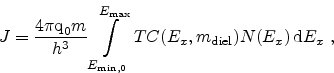 |
(5.1) |
where  is the electron mass in silicon and
 the electron mass in the
dielectric [68].
the electron mass in the
dielectric [68].
 is the transmission
coefficient and
is the transmission
coefficient and
 the supply function which is given as
 |
(5.2) |
Here,  and
and  denote the energy distribution functions near the
interfaces [69].
denote the energy distribution functions near the
interfaces [69].
The energy band conditions for Fowler-Nordheim tunneling, which is a special
case of direct tunneling, are depicted in Figure 5.4(b). The
electrons do not tunnel directly to the other side of the barrier. Instead
they tunnel from the silicon inversion layer to the conduction band of the
layer from where they are transported to the gate contact. The
Fowler-Nordheim regime is significant for thicker dielectrics and sufficiently
high electric fields.
A thorough investigation of modeling and simulation of tunneling mechanisms can
be found in the thesis of Gehring [69].
5.3.2 Trap-Assisted Tunneling
As the reduction of the applied voltages does not keep up with the
miniaturization of actual devices the electric fields across dielectric layers
are constantly increasing. Especially for non-volatile memory cells high
electric fields are necessary in order to achieve quick write and erase cycles.
Due to the repeated high-field stress, defects can arise in the dielectric
leading to tunneling currents, even at low fields. This stress-induced leakage
current (SILC) [70,71] plays a major role in the
determination of the retention times of non-volatile memory cells.
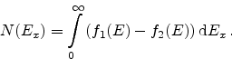
There are many approaches to model trap-assisted tunneling (TAT). One is to
model the defect assisted tunneling process including a single trap. For each
trap position tunneling from the cathode to the trap and further to the anode
is considered. From this the trap occupancy function can be calculated which
is used to compute the tunneling current [72]. This single-TAT
approach works very well for slightly degraded devices or devices with thin
gate dielectrics. For thicker dielectrics with a high defect density it is
reasonable to assume that also the interaction of two or more traps in the
tunneling process takes place [73].
For the modeling of multi-trap assisted tunneling (multi-TAT) approaches like a
two-trap process [74,75] or a multi-trap process
considering hopping of carriers between distinct defects [76] have
been presented. Recently, anomalous charge loss in floating-gate memory cells
has been reported [73], where a two-trap model was used to
reproduce the measured data.
For correct modeling of such highly degraded devices a new approach is proposed
as part of this work. It rigorously computes TAT current assisted by multiple
traps [77,78]. In this model hopping
processes between all oxide defects are taken into account. In addition the
filling of oxide traps with carriers, leading to space charge in the oxide and
therefore to a shift of the threshold voltage, is accounted for. This shift
can lead to circuit failure as the timing parameters of the device are
degraded.
The model for the simulation of SILC in highly degraded devices is based on
inelastic, phonon-assisted tunneling [79] with the tunneling-rate
proposed by Herrmann and Schenk [72]. These approaches are
extended for modeling the interaction of multiple traps in the tunneling
process.
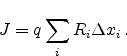
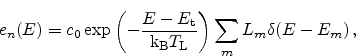
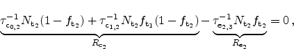
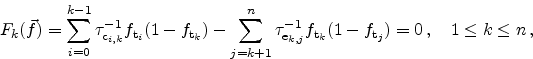
Figure 5.5:
Inelastic tunneling process including a sole trap. The excess
energy of the tunneling electron is released by means of phonon emission.
|
|
The defect-assisted tunneling process of an electron from the cathode to the
anode via a trap is considered as a two-step process. Electrons are captured
from the cathode, relax to the energy level of the trap by emitting one or more
phonons with the energy  , and are then emitted to the anode. This
process is inelastic as the electron energy is not conserved during the
tunneling process. Figure 5.5 depicts this process
including the phonon emission.
, and are then emitted to the anode. This
process is inelastic as the electron energy is not conserved during the
tunneling process. Figure 5.5 depicts this process
including the phonon emission.
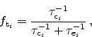
In the single-trap assisted tunneling approach the tunneling current for each
trap is calculated separately. The total tunneling current is afterwards
superimposed from the individual contributions. Although the interaction
between neighboring traps is of importance in highly degraded dielectrics
(Section 5.3.2.3), for less degraded devices this approach can be
used [72,80].
The tunneling current density is modeled as the sum of capture or emission
rates of each trap,
 or
or
 , which are equal in the stationary case,
 , multiplied by the trap cross section
  ,
,
 |
(5.3) |
The energetic position of the trap,  , with respect to the
conduction band edge determines the trap cross section [81]
, with respect to the
conduction band edge determines the trap cross section [81]
 |
(5.4) |
where
 denotes the electron mass in the dielectric, which is used
as a model calibration parameter.
denotes the electron mass in the dielectric, which is used
as a model calibration parameter.
The single-TAT and the multi-TAT models differ in the way the capture and
emission rates are calculated. When only single-trap processes are considered
(see Figure 5.5) the rates are determined
by [72]
 |
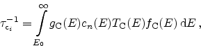
(5.5) |
 |
(5.6) |
Here,
 and
and
 are the capture and emission times and
 is the
trap concentration. As the capture and emission rates are equal in the
stationary case, the trap occupancy
is the
trap concentration. As the capture and emission rates are equal in the
stationary case, the trap occupancy
 can be directly calculated as
 |
(5.7) |
where the inverse capture and emission times are defined as
as [72,82]
 |
(5.8) |
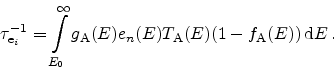 |
(5.9) |
In these expressions,
 and
and
 denote the density
of states in the cathode and anode, respectively,
denote the density
of states in the cathode and anode, respectively,
 and
and
 the
transmission coefficients from the cathode and the anode, and the symbols
the
transmission coefficients from the cathode and the anode, and the symbols  and
and  are computed as
 |
(5.10) |
 |
(5.11) |
with
 |
(5.12) |
 |
(5.13) |
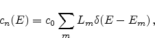
The summation index gives the number of discrete phonon emissions,
 is the phonon energy, and
  is the multiphonon transition
probability [72]. The symbols
is the multiphonon transition
probability [72]. The symbols
 and
and
 represent
the Fermi-distributions,
represent
the Fermi-distributions,  the electric field in the dielectric, and
 the band gap of
. The transmission coefficients
were evaluated by a numerical WKB method which yields reasonable accuracy for
single-layer dielectrics. This model has been used in a more or less similar
form by various authors [80,79,82].
the band gap of
. The transmission coefficients
were evaluated by a numerical WKB method which yields reasonable accuracy for
single-layer dielectrics. This model has been used in a more or less similar
form by various authors [80,79,82].
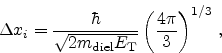
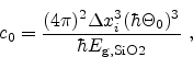
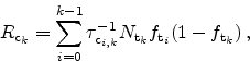
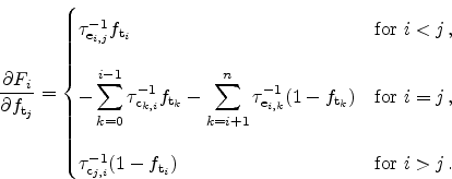
Figure 5.6:
Multi-trap assisted tunneling process. The tunneling rate  of a
specific trap is determined by all capture and emission times to and from
the trap.
of a
specific trap is determined by all capture and emission times to and from
the trap.
|
|
5.3.2.3 Multi-Trap Assisted Tunneling
For highly degraded devices the isolated calculation for each trap is not
sufficient anymore [74]. Anomalous charge loss in memory cells
has been observed and was explained by conduction through a second
trap [74]. The single-trap model can be extended for this case,
and the rate equations become (see Figure 5.6)
 |
(5.14) |
 |
(5.15) |
where instantaneous transitions between occupied and free traps are assumed.
For thicker dielectrics it is quite reasonable to assume that an arbitrary
number of traps assist in the conduction process. We therefore extend the
model to  traps where the capture and emission rates are evaluated as
 |
(5.16) |
 |
(5.17) |
The values for
 and
and
 , which are the trap occupation
probabilities at the cathode and the anode, are set to 1 and 0,
respectively. This way the cathode acts as a perfect electron source and the
anode as an electron sink.
, which are the trap occupation
probabilities at the cathode and the anode, are set to 1 and 0,
respectively. This way the cathode acts as a perfect electron source and the
anode as an electron sink.
From the capture and emission rates the following equation system can be set up
 |
(5.18) |
from which the values of all trap occupation probabilities have to be
calculated. This is performed using a Newton method with the cost function
 for a trap at position
 |
(5.19) |
and the values of the derivatives in the Jacobian matrix
 |
(5.20) |
A typical number of unknowns of the equation system is 15. Depending on the
dielectric thickness and trap energy the result does not improve when further
increasing this number. The computational effort remains negligible compared
to the total device simulation time. The multi-trap assisted tunneling current
density can then be obtained from the capture or emission rates
![\begin{displaymath}
J = q \sum_{i}
\left[
\sum_{j=0}^{i-1} \tau\ensuremath{_{...
...remath{f_{\textrm{t$_\mathit{i}$}}})
\right]
\Delta x_i .
\end{displaymath}](img476.png) |
(5.21) |
By coupling this model to the semiconductor device equations
(Section 2.1) the simulation of the effect of charged defects on
the threshold voltage of memory devices is possible. The space charge density
in the dielectric is calculated from the trap occupation function as
 |
(5.22) |
and added to Poisson's equation as described in Section 2.1.2 with
 |
(5.23) |
The trapped electrons shift the threshold voltage to more positive voltages and
can lead to circuit failure.
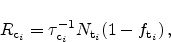
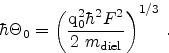
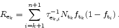
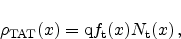
Figure 5.7:
The formation of traps randomly distributed across the oxide of an
MOS structure as simulated using Minimos-NT. Each trap contributes to
additional tunneling current.
|
|
The implementation of these models into the device- and circuit-simulator
Minimos-NT [44] allows the two- and three-dimensional study of
single- and multi-trap assisted tunneling as well as direct tunneling
mechanisms. Figure 5.7 gives an example of a highly degraded
dielectric with traps randomly distributed across the oxide. The dielectric
can now be used for the simulation of multi-trap assisted tunneling.
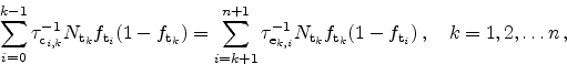
Figure 5.8:
(a) SILC simulations for a set of MOS devices at 1 V gate bias. The
oxide was assumed to have a constant trap concentration. The multi-TAT
current is always larger than the single-TAT current. (b) The trap
occupancy
 in the oxide of a 1.5 nm MOS transistor at 1 V gate
bias.
in the oxide of a 1.5 nm MOS transistor at 1 V gate
bias.
![\includegraphics[width=0.495\textwidth]{figures/compare-oxides}](img480.png)
Oxide thickness variation
|
![\includegraphics[width=0.495\textwidth]{figures/compare-fts}](img481.png)
Trap occupancy along the channel
|
|
Figure 5.8(a) shows a comparison of SILC simulation results assuming
three different tunneling mechanisms, namely direct tunneling, single-TAT, and
multi-TAT. The models have been applied to a set of MOS transistors with gate
dielectric thicknesses ranging from 1.5nm up to 9nm. The gate is biased at
1V, source and drain are kept at 0V. For both, the single-TAT and the
multi-TAT simulations, the trap energy is set to 2.8eV below the dielectric
conduction band with a constant trap density of
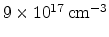 across the oxide.
In the multi-trap simulation the tunneling current is several orders of
magnitude higher than in the single-trap simulation. This is due to the fact
that the multi-TAT current includes the single-TAT component as a limiting
case. The multi-TAT model considers the capture and emission processes from
the cathode and to the anode, respectively, and also the capture and emission
processes involving all other trap centers. This leads to the comparably high
multi-TAT component in devices with thicker oxides. It has to be considered,
though, that this high current is mainly due to the assumption of uniformly
distributed trap concentrations across the oxide, which implies that the total
amount of traps is much higher in thick dielectrics. The direct tunneling
component loses importance for thicker dielectrics but dominates for thin
dielectrics as found in logic CMOS devices. For devices with thicker oxides
and higher trap densities multi-TAT processes become increasingly important.
Figure 5.8(b) depicts the resulting trap occupancy within the oxide. An
MOS transistor with 1V gate bias was simulated. It can be seen that the trap
occupancy
 is remarkably lower in the multi-TAT case. The reason is
the higher probability for electrons to tunnel to one of the neighbor traps
compared to tunneling to the anode as it is the only possibility in the
single-TAT model.
is remarkably lower in the multi-TAT case. The reason is
the higher probability for electrons to tunnel to one of the neighbor traps
compared to tunneling to the anode as it is the only possibility in the
single-TAT model.
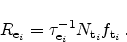
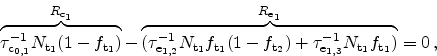
Figure 5.9 outlines the threshold voltage
 for different oxide
thicknesses. The direct tunneling model, applying the commonly used Tsu-Esaki
approach, does not account for the filling of traps in the oxide. Therefore the
threshold voltage is not shifted compared to the simulation without a tunneling
model. The new multi-TAT model predicts an increase in
. This higher
threshold voltage is due to the filled and therefore negatively charged traps.
for different oxide
thicknesses. The direct tunneling model, applying the commonly used Tsu-Esaki
approach, does not account for the filling of traps in the oxide. Therefore the
threshold voltage is not shifted compared to the simulation without a tunneling
model. The new multi-TAT model predicts an increase in
. This higher
threshold voltage is due to the filled and therefore negatively charged traps.
For thicker dielectrics with high defect density the inclusion of multiple
traps is crucial for the simulation of both, quantum mechanical gate currents
and the shift of threshold voltages. Thin dielectrics, on the other hand side,
may be as well treated using the single-TAT model.
Figure 5.9:
Comparison of the threshold voltage
of MOSFET structures with
different oxide thicknesses. Thicker devices suffer from a higher shift
due to the availability of more trapped charges.
|
|
Next: 6. Negative Bias Temperature
Up: 5. Dielectric Degradation and
Previous: 5.2 Dielectric Wearout and
R. Entner: Modeling and Simulation of Negative Bias Temperature Instability
![\includegraphics[width=10cm]{figures/banddiagram-traps-phononemission-color}](img431.png)
![\includegraphics[width=10cm]{figures/banddiagram-traps-double-color}](img465.png)
![\includegraphics[width=12cm]{figures/traps6_rot.eps}](img479.png)
![\includegraphics[width=\figwidth]{figures/compare-vt}](img484.png)