Next: 2.1.1 Molecular Structure of Up: 2. Silicon Oxidation Techniques Previous: 2. Silicon Oxidation Techniques
The growth of silicon dioxide is one of the most important processes in the fabrication of MOS transistors [175].
The attributes of SiO![]() which make it appealing for the semiconductor industry are [80,175]:
which make it appealing for the semiconductor industry are [80,175]:
Table 2.1 shows some important properties of silicon dioxide [47]. It can be noted that
oxides grown in a dry atmosphere have a higher density, which implies less impurities and a better quality oxide than when
grown in a wet atmosphere. Thermal expansion refers to the oxide's volume expansion or shrinkage, when exposed to a
range of temperatures. For oxides, the thermal expansion coefficient is very low, meaning it does not exert much stress and strain
on other materials which are in contact with it. Young's modulus and Poisson's ratio measure the oxide's stiffness and its
negative ratio of transverse to axial strain, respectively, which are important measures of a material's mechanical stability.
The thermal conductivity, which varies for thin sputtered (1.1W![]() m-K), thin thermally grown (1.3W
m-K), thin thermally grown (1.3W![]() m-K), and bulk (1.4W
m-K), and bulk (1.4W![]() m-K)
oxides is an important parameter which affects power during operation [25]. It is also found that the thermal conductivity
of oxides changes depending on the oxide thickness [25]. The high dielectric strength shows the stability of SiO
m-K)
oxides is an important parameter which affects power during operation [25]. It is also found that the thermal conductivity
of oxides changes depending on the oxide thickness [25]. The high dielectric strength shows the stability of SiO![]() under
high electric fields, suggesting that the oxide film is very suitable for dielectric isolation.
under
high electric fields, suggesting that the oxide film is very suitable for dielectric isolation.
The silicon dioxide molecule can be described as a three-dimensional network of tetrahedra cells, with four oxygen
atoms surrounding each silicon ion, shown in Figure 2.2a. The length of a Si-O bond is 0.162nm, while the
normal distance between two oxide bonds is 0.262nm. The Si-Si bond distance depends on the SiO![]() arrangement,
but is approximately 0.31nm and the bond angle O-Si-O is approximately 109
arrangement,
but is approximately 0.31nm and the bond angle O-Si-O is approximately 109
![]() .
The bond angle Si-O-Si is ideally approximately 145
.
The bond angle Si-O-Si is ideally approximately 145
![]() , but it can vary between 100
, but it can vary between 100
![]() and 170
and 170
![]() with minimal change in bond energy.
The tetrahedral form is the basic unit from which a SiO
with minimal change in bond energy.
The tetrahedral form is the basic unit from which a SiO![]() structure is formed, even
though SiO
structure is formed, even
though SiO![]() can exist in a crystalline structure. The reason for the amorphous oxide structure is the absence of any
crystalline form of SiO
can exist in a crystalline structure. The reason for the amorphous oxide structure is the absence of any
crystalline form of SiO![]() whose lattice size closely matches the silicon lattice [175]. The tetrahedra bond together by
sharing oxygen atoms as illustrated in Figure 2.2b in a sample six-membered ring.
whose lattice size closely matches the silicon lattice [175]. The tetrahedra bond together by
sharing oxygen atoms as illustrated in Figure 2.2b in a sample six-membered ring.
|
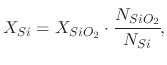
From the above analysis, it can be concluded that, as the oxide grows, it consumes the silicon atoms at the surface of the wafer. This causes the silicon-silicon dioxide interface to move into the wafer while the oxide grows. The equation which governs the amount of consumed silicon is
 |
(27) |
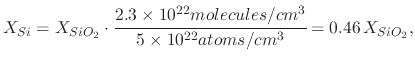 |
(28) |
Therefore approximately 46% of the silicon dioxide which is grown on a silicon wafer is found within the bounds of the original silicon, while approximately 54% is new volume, which grows into the ambient. Figure 2.3 shows the location of the original silicon surface followed by the oxide-silicon and oxide-ambient interfaces after an oxidation step.
![\includegraphics[width=0.41\linewidth]{chapter_oxidation/figures/molecule.eps}](img142.png)
![\includegraphics[width=0.55\linewidth]{chapter_oxidation/figures/structure.eps}](img143.png)
![\includegraphics[width=0.48\linewidth]{chapter_oxidation/figures/Silicon.eps}](img150.png)
![\includegraphics[width=0.48\linewidth]{chapter_oxidation/figures/Oxide.eps}](img151.png)