5.2 The Level Shift Model
So far, only qualitative statements about the defect behavior could be made based on
the switching levels. In order to make quantitative predictions, the ETM
must be generalized in a way to account for the levels shift. Recall that the
conventional concept of the ETM is based on the assumption that the energy levels
for tunneling ‘into’ and ‘out of’ a defect coincide. This is only the case for
unrealistic defects which do not deform after a tunneling event. But as proven
in the previous Section 5.1, defects do undergo structural relaxation and
therefore feature two switching levels, say  for hole capture and
  for
hole emission for instance, which can even be separated by some electron
Volts (see Fig. 5.9). To be precise, the switching levels
for
hole emission for instance, which can even be separated by some electron
Volts (see Fig. 5.9). To be precise, the switching levels  and
and  actually originate from the one defect orbital and thus must be correctly
interpreted as one trap level, which shifts after each charging or discharging event.
For the trapping kinetics, this means that only one of these levels can be
present in the band diagram at a time. For instance, when the defect in
Fig. 5.10 is in its neutral charge state, it has a trap level
actually originate from the one defect orbital and thus must be correctly
interpreted as one trap level, which shifts after each charging or discharging event.
For the trapping kinetics, this means that only one of these levels can be
present in the band diagram at a time. For instance, when the defect in
Fig. 5.10 is in its neutral charge state, it has a trap level  for hole
capture while its corresponding trap level
for hole
capture while its corresponding trap level  remains inactive for the time
being. If a hole capture process takes place, the
remains inactive for the time
being. If a hole capture process takes place, the  level vanishes and
thus the
level vanishes and
thus the  level appears. Based on the considerations above, the ETM
must be regarded as a special case of the level shift model (LSM) but with a
negligible defect relaxation. Consequently, the formulation of the ETM must be
modified in order to account for the level shift. Thus equation (4.6) is rewritten
as
level appears. Based on the considerations above, the ETM
must be regarded as a special case of the level shift model (LSM) but with a
negligible defect relaxation. Consequently, the formulation of the ETM must be
modified in order to account for the level shift. Thus equation (4.6) is rewritten
as
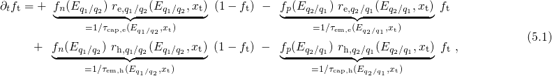
where the rates are defined as
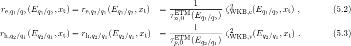
 and
and  denote the two charge states involved in the tunneling process and the
trap levels
denote the two charge states involved in the tunneling process and the
trap levels  and
and  corresponds to the switching traps introduced in
Section 2.3. The above rate equation is reminiscent of the ETM presented in the
previous Section 2.5.2. The peculiarity of the LSM is that the particular terms on
the right-hand side of equation (5.1) must be evaluated for different energies, namely
corresponds to the switching traps introduced in
Section 2.3. The above rate equation is reminiscent of the ETM presented in the
previous Section 2.5.2. The peculiarity of the LSM is that the particular terms on
the right-hand side of equation (5.1) must be evaluated for different energies, namely
 or
or  , depending on the charge state of the defect before the
tunneling transition occurs. For instance, the positively charged defect of
Fig. 5.9 has a trap level
, depending on the charge state of the defect before the
tunneling transition occurs. For instance, the positively charged defect of
Fig. 5.9 has a trap level  , which must be applied for calculation of the
electron capture rate
, which must be applied for calculation of the
electron capture rate 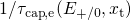 (see Fig. 5.10). By contrast, the
neutralized defect features a trap level
(see Fig. 5.10). By contrast, the
neutralized defect features a trap level  used for the hole capture rate
 . The calculation of the corresponding time constants is illustrated
in Fig. 5.10. It is important to note here that the expressions for
. The calculation of the corresponding time constants is illustrated
in Fig. 5.10. It is important to note here that the expressions for  ,
,  ,
,
 , and
, and  remain the ‘same’ as in the ETM and only change in the
energy they are evaluated for. This is due to the fact that the tunneling
mechanism itself is not affected by the structural relaxation. Thus, analogously to
the ETM, the tunneling process can be described by the tunneling rates
(2.45) and (2.46) of the ETM and reasonably approximated by (5.2) and
(5.3).
remain the ‘same’ as in the ETM and only change in the
energy they are evaluated for. This is due to the fact that the tunneling
mechanism itself is not affected by the structural relaxation. Thus, analogously to
the ETM, the tunneling process can be described by the tunneling rates
(2.45) and (2.46) of the ETM and reasonably approximated by (5.2) and
(5.3).
In the following, a new quantity, referred to as the demarcation
energy,
 will be introduced. It determines equilibrium occupancy of the defects and is
defined by the condition
will be introduced. It determines equilibrium occupancy of the defects and is
defined by the condition
with
Assuming Boltzmann statistics, the energy dependences of the electron and hole
occupation can be approximated as follows: Suppose that  and
and  as it has been the case for the
  center. Then only the exponential terms of
  and
and  enter the time constants.
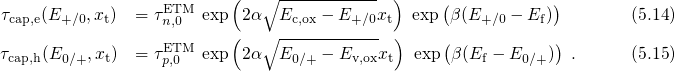
The WKB factors in the expressions (5.5) and (5.6) can be replaced by their
approximative variants for a rectangular barrier. Since
enter the time constants.
The WKB factors in the expressions (5.5) and (5.6) can be replaced by their
approximative variants for a rectangular barrier. Since  holds, equation (5.4) can be
rewritten as Taking the logarithm of this equation and after rearranging some terms, one obtains
with The factor
holds, equation (5.4) can be
rewritten as Taking the logarithm of this equation and after rearranging some terms, one obtains
with The factor  in equation (5.11) takes a value of approximately
  at
room temperature (
at
room temperature ( ). Thus the last term is negligible compared to the
remainder of equation (5.11) and
). Thus the last term is negligible compared to the
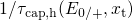
remainder of equation (5.11) and  can be estimated by This quantity predicts the electron occupancy of a defect when equilibrium has been
reached. For instance, when a stress voltage is applied to the gate of a pMOSFET,
can be estimated by This quantity predicts the electron occupancy of a defect when equilibrium has been
reached. For instance, when a stress voltage is applied to the gate of a pMOSFET,
 is raised above
  and the initially neutral defect can capture a substrate hole
during the stress phase. Conversely, when the MOSFET is switched from stress to
relaxation,
and the initially neutral defect can capture a substrate hole
during the stress phase. Conversely, when the MOSFET is switched from stress to
relaxation,  falls below
  and the positively charged defect will become
neutralized in equilibrium. As an example, the
and the positively charged defect will become
neutralized in equilibrium. As an example, the  level of the oxygen vacancy varies
between
level of the oxygen vacancy varies
between  and
and  according to the present DFT results. These values
lie too low to be shifted above
according to the present DFT results. These values
lie too low to be shifted above  for defects located close to the interface
(
for defects located close to the interface
( ). Therefore, the level
  of the
  center reveals that the LSM is
incompatible with the concept of hole capture into oxygen vacancies. All other
defect candidates, investigated by the DFT simulations in this thesis, feature
values of
center reveals that the LSM is
incompatible with the concept of hole capture into oxygen vacancies. All other
defect candidates, investigated by the DFT simulations in this thesis, feature
values of  close to
  and cannot be ruled out on the basis of the above
argument.
and cannot be ruled out on the basis of the above
argument.
While the equilibrium occupation of the defects is given by the demarcation energy,
the trapping dynamics directly follow from the electron and hole capture time
constants, whose dependence on the Fermi level and the trap depth will be discussed
in the following. The ‘interesting’ instance is when the Fermi level is situated
inbetween the levels  and
and  (cf. Fig. 5.10). Using Boltzmann statistics
(5.7) and (5.8) and approximative WKB factor (5.9), the capture time constants can
be estimated by
(cf. Fig. 5.10). Using Boltzmann statistics
(5.7) and (5.8) and approximative WKB factor (5.9), the capture time constants can
be estimated by
In the equations above, the last term, originating from the Fermi-Dirac distribution,
has the largest impact on both time constants. For instance,  exponentially
depends on the energy difference
exponentially
depends on the energy difference  , that is, a higher
  level
gives a larger
level
gives a larger  . Analogous considerations hold true for the energy
difference
. Analogous considerations hold true for the energy
difference  and
and  . These dependences are also reflected in the
exponential branches of the time constant plot in Fig. 5.10. Note that the
simulated defect in this figure has been placed only
. These dependences are also reflected in the
exponential branches of the time constant plot in Fig. 5.10. Note that the
simulated defect in this figure has been placed only  away from the
interface where the time taken for the tunnel step can be almost neglected.
However, when the defects are assumed to be situated deeper within the oxide,
their time constants are increased due to the reduced tunnel probability. As
demonstrated in Fig. 5.11 (left), this effect is more pronounced in the middle
of the oxide bandgap while it almost diminishes towards the band edges
due to the reduced tunneling barrier there. The ‘uninteresting’ instance is
when the Fermi level is situated above
away from the
interface where the time taken for the tunnel step can be almost neglected.
However, when the defects are assumed to be situated deeper within the oxide,
their time constants are increased due to the reduced tunnel probability. As
demonstrated in Fig. 5.11 (left), this effect is more pronounced in the middle
of the oxide bandgap while it almost diminishes towards the band edges
due to the reduced tunneling barrier there. The ‘uninteresting’ instance is
when the Fermi level is situated above  as well as
  as shown
Fig. 5.11 (right). In this case
as shown
Fig. 5.11 (right). In this case  is larger than
  , implying that hole
capture is effectively suppressed. Note that analogous consideration holds
true for the electron capture when the Fermi level fall below
, implying that hole
capture is effectively suppressed. Note that analogous consideration holds
true for the electron capture when the Fermi level fall below  and
and
 .
.
5.2.1 Model Evaluation
In this section, the LSM will be employed to investigate the impact of the level
shift on the trapping dynamics in NBTI experiments. Based on the NBTI
checklist established in Section 1.4, it will be tested whether this model is
capable of reproducing the NBTI degradation seen in experiments. The
following simulations are carried out on a pMOSFET ( )
with a strongly doped p-poly gate (
)
with a strongly doped p-poly gate ( ). The thickness of
the oxide layer has been chosen to be
). The thickness of
the oxide layer has been chosen to be  for demonstration purposes.
Thereby, the traps can be homogeneously spread within the dielectric but
are still sufficiently separated (
for demonstration purposes.
Thereby, the traps can be homogeneously spread within the dielectric but
are still sufficiently separated ( ) from the poly interface in order to
be able to neglect trapping from the gate. Furthermore, this wide range
of trap depths ensures a large distribution of capture and emission times
over 14 decades in time (cf. Fig. 5.11). The energy levels of the traps have
been assumed to be uniformly distributed with the
) from the poly interface in order to
be able to neglect trapping from the gate. Furthermore, this wide range
of trap depths ensures a large distribution of capture and emission times
over 14 decades in time (cf. Fig. 5.11). The energy levels of the traps have
been assumed to be uniformly distributed with the  and the
  levels being uncorrelated and thus independently calculated using a random
number generator. The operation temperature is set to
levels being uncorrelated and thus independently calculated using a random
number generator. The operation temperature is set to  and thus lies
in the middle of the range relevant for NBTI. It is noted that only charge
injection from the substrate is accounted for in the following simulations for
simplicity.
and thus lies
in the middle of the range relevant for NBTI. It is noted that only charge
injection from the substrate is accounted for in the following simulations for
simplicity.
In the following, the basic properties of the LSM will be discussed on the basis of a
simple showcase. Therefore, this model is evaluated for a type of defect whose trap
level  has a wide distribution below
  while the
  counterpart
is sharply peaked slightly above
counterpart
is sharply peaked slightly above  (see Fig. 5.12). At the beginning of
the stress phase nearly all defects are neutral and thus occupied by one
electron. In this state, the traps are characterized by the hole capture levels
(see Fig. 5.12). At the beginning of
the stress phase nearly all defects are neutral and thus occupied by one
electron. In this state, the traps are characterized by the hole capture levels
 located below the substrate valence band. The corresponding electron
capture levels
located below the substrate valence band. The corresponding electron
capture levels  lie above the substrate conduction band but are inactive
for the time being. During the stress phase, the substrate holes must be
thermally excited to the defect level
lie above the substrate conduction band but are inactive
for the time being. During the stress phase, the substrate holes must be
thermally excited to the defect level  in order that a tunneling process can
occur. In equation (5.6) their energy-dependent concentration is linked to the
factor
in order that a tunneling process can
occur. In equation (5.6) their energy-dependent concentration is linked to the
factor  , which decays exponentially with decreasing energies assuming
Boltzmann statistics. This decay would lead to a temporal filling of traps from
energetically higher towards lower traps in the band diagram. Furthermore, the
tunneling of electrons and holes has an additional trap depth dependence,
which is reflected in the WKB factor of equation (5.6). Analogously to the
ETM, this would cause a temporal filling of traps starting from close to the
interface and continuing deep into the oxide. As demonstrated in Fig. 5.13, the
superposition of both effects results in a tunneling hole front which proceeds
from high defect levels close to the interface towards lower ones deep in the
oxide. The resulting time evolution of the trap occupancies is visualized in
Fig. 5.12.
, which decays exponentially with decreasing energies assuming
Boltzmann statistics. This decay would lead to a temporal filling of traps from
energetically higher towards lower traps in the band diagram. Furthermore, the
tunneling of electrons and holes has an additional trap depth dependence,
which is reflected in the WKB factor of equation (5.6). Analogously to the
ETM, this would cause a temporal filling of traps starting from close to the
interface and continuing deep into the oxide. As demonstrated in Fig. 5.13, the
superposition of both effects results in a tunneling hole front which proceeds
from high defect levels close to the interface towards lower ones deep in the
oxide. The resulting time evolution of the trap occupancies is visualized in
Fig. 5.12.
The temporal filling is also reflected in the occupancies of the demarcation energies,
shown in Fig. 5.14. As already mentioned before, only defects located above  can
participate in hole capture. As a consequence, the temporal filling of traps does
not proceed below
can
participate in hole capture. As a consequence, the temporal filling of traps does
not proceed below  , which thus marks a border to the tunneling hole
front.
, which thus marks a border to the tunneling hole
front.
After the stress phase, a large part of the hole capture levels has disappeared and is
replaced by their corresponding electron capture levels  . The latter
are assumed to be concentrated in a small trap band slightly above the
substrate conduction band. During the recovery phase, electrons in the substrate
conduction band must be thermally excited up to the
. The latter
are assumed to be concentrated in a small trap band slightly above the
substrate conduction band. During the recovery phase, electrons in the substrate
conduction band must be thermally excited up to the  level where
the trap depth-dependent tunneling process can take place. According to
Fig. 5.12, the defects are found to be filled according to their trap depth, visible
as a horizontally moving tunnel front. The small separation of the
level where
the trap depth-dependent tunneling process can take place. According to
Fig. 5.12, the defects are found to be filled according to their trap depth, visible
as a horizontally moving tunnel front. The small separation of the  levels on the energy scale results in a narrow distribution of electron capture
times. From this it follows that two particular charging events at the upper
and the lower edge of the trap band can be hardly resolved in time. As a
consequence, no vertical component in the motion of the tunnel front is observed
during the recovery phase of Fig. 5.12. Analogously to the stress phase, the
tunneling hole front also appears in the occupancies of the demarcation
levels displayed in Fig. 5.14. During the relaxation phase, the
levels on the energy scale results in a narrow distribution of electron capture
times. From this it follows that two particular charging events at the upper
and the lower edge of the trap band can be hardly resolved in time. As a
consequence, no vertical component in the motion of the tunnel front is observed
during the recovery phase of Fig. 5.12. Analogously to the stress phase, the
tunneling hole front also appears in the occupancies of the demarcation
levels displayed in Fig. 5.14. During the relaxation phase, the  levels are
shifted below
levels are
shifted below  where they can be neutralized if equilibrium has been
reached. However, Fig. 5.14 reveals that the discharging of traps has not been
completed even until an unrealistic long relaxation time of
where they can be neutralized if equilibrium has been
reached. However, Fig. 5.14 reveals that the discharging of traps has not been
completed even until an unrealistic long relaxation time of  . It is important
to note here that
. It is important
to note here that  during stress and relaxation determines the active
area in which hole capture is possible. Defects above this area are already
unoccupied before stress and thus cannot capture a further hole, while the
ones below will remain neutral due to the high hole emission rate. As a
result, only defects within this area can change their charge state and thus
contribute to the net amount of captured holes and in further consequence to
NBTI.
during stress and relaxation determines the active
area in which hole capture is possible. Defects above this area are already
unoccupied before stress and thus cannot capture a further hole, while the
ones below will remain neutral due to the high hole emission rate. As a
result, only defects within this area can change their charge state and thus
contribute to the net amount of captured holes and in further consequence to
NBTI.
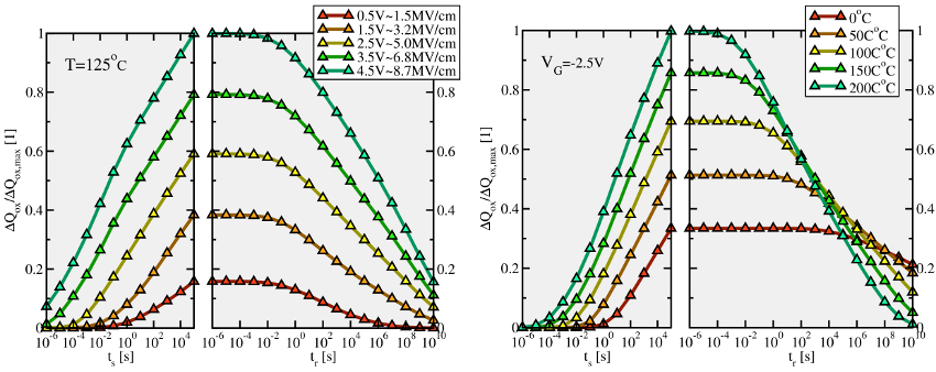
The LSM has been employed to simulate NBTI degradation in a pMOSFET for a
wide range of different stress conditions. The calculated stress/relaxation curves for
the aforementioned showcase are presented in Fig. 5.15. In contrast to the ETM,
they exhibit a marked temperature dependence in addition to the obvious field
acceleration. While the former one mainly stems from the temperature dependent
Fermi-Dirac distribution in  (cf. equation (5.6)), the latter one cannot be
simply interpreted by the lowering of the tunneling barrier at higher
(cf. equation (5.6)), the latter one cannot be
simply interpreted by the lowering of the tunneling barrier at higher  . The
field acceleration originates form the larger shift of the trap levels at higher
. The
field acceleration originates form the larger shift of the trap levels at higher
 , as visualized in Fig. 5.16. As such, the field acceleration strongly
depends on the distribution of the trap levels in space and energy but is
not inherent to the LSM itself. For instance, a defect with
, as visualized in Fig. 5.16. As such, the field acceleration strongly
depends on the distribution of the trap levels in space and energy but is
not inherent to the LSM itself. For instance, a defect with  and
and
 during stress will not be able to capture a hole at all (see Fig. 5.17).
In order to obtain more realistic results, tunneling from interface states [23] has been
incorporated into LSM. The obtained degradation curves for defects with
 and
and  are depicted in Fig. 5.18.
Based on these results, it will be evaluated whether the LSM can satisfactorily
reproduce the basic features seen in NBTI experiments. In the NBTI checklist of
Table 5.2, these features are formulated as necessary criteria, where each of them will
be judged in the following.
are depicted in Fig. 5.18.
Based on these results, it will be evaluated whether the LSM can satisfactorily
reproduce the basic features seen in NBTI experiments. In the NBTI checklist of
Table 5.2, these features are formulated as necessary criteria, where each of them will
be judged in the following.
- Hole trapping during stress and relaxation is found to cover the time range
from milliseconds to a few thousand seconds as in the reference data of
Section 1.4. Moreover, it even extends from
 to
to  during stress
and from
during stress
and from  to
to  during relaxation and thus even goes far beyond
the experimental time window.
during relaxation and thus even goes far beyond
the experimental time window.
- At low stress voltages, the degradation curves feature only a weak
curvature and thus roughly follow a logarithmic time behavior.
- Only small deviations from the logarithmic time behavior are present at
low stress voltages in the relaxation phase. But one should kept in mind
that the relaxation data cannot be scaled as there is an intersection point
between the high and low temperature recovery curves.
- Since the degradation accumulated during the stress phase does not
completely recover during the much longer relaxation phase, the LSM
allows for the asymmetry between stress and relaxation. This can be
ascribed to the fact that the
 levels are more widely spread on the
energy scale than their
levels are more widely spread on the
energy scale than their  counterparts. The wide separation of the
 levels is linked to a broad distribution of
  , giving rise to a
retarded recovery.
, giving rise to a
retarded recovery.
- The field acceleration is found to follow a nearly linear behavior (cf.
Fig. 5.19), which is inconsistent with the NBTI criteria of Section 1.4.
- The elevated temperatures yield a weakly enhanced NBTI degradation
during stress (cf. Fig. 5.19), while they reduce the electron capture
times and thus lead to an accelerated recovery during relaxation. These
tendencies cannot be reconciled with the quadratic temperature activation
obtained in experiments.
The above list provides strong evidence that the LSM cannot be reconciled with the
experimental NBTI data. As a consequence, pure tunneling must be discarded as a
possible cause for hole trapping in NBTI.
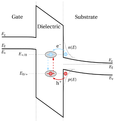
 and
and  for
electron and hole capture, respectively. When the positively charged trap (blue
filled circle in gray ellipse) captures a substrate electron with an energy of
for
electron and hole capture, respectively. When the positively charged trap (blue
filled circle in gray ellipse) captures a substrate electron with an energy of  (blue arrow), the defect level
  vanishes but reappears at
  . The now
neutral defect (red circle in gray ellipse) is only capable of capturing a hole from
the silicon valence band (red arrow). Right after this process the defect level
has returned to its initial position
. The now
neutral defect (red circle in gray ellipse) is only capable of capturing a hole from
the silicon valence band (red arrow). Right after this process the defect level
has returned to its initial position  again.
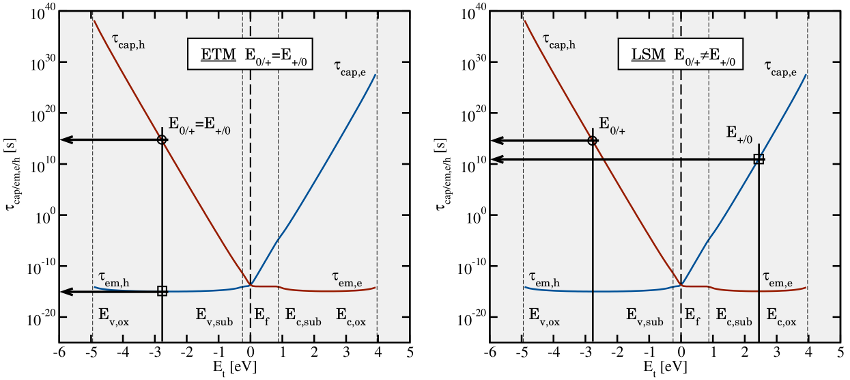
 ). The defect is placed close to the interface (
 ) of a
pMOSFET in the off-state and features one single trap level
) of a
pMOSFET in the off-state and features one single trap level  indicated by the vertical dashed line. In the present case, the trap level lies
 below the substrate valence band edge, where hole emission (circle)
proceeds much faster than hole capture (box). Note that for trap levels within
the substrate bandgap also tunneling from interface states
below the substrate valence band edge, where hole emission (circle)
proceeds much faster than hole capture (box). Note that for trap levels within
the substrate bandgap also tunneling from interface states  at which electron capture time is calculated
has been changed (
at which electron capture time is calculated
has been changed ( ). According to the equations (
 and
and  are evaluated at two different trap levels, namely one at
 for electron capture and another at
  for hole capture. For this case
the relative magnitude of
for hole capture. For this case
the relative magnitude of  and
and  depends on the energy distance of
the respective trap level to
depends on the energy distance of
the respective trap level to  .
.


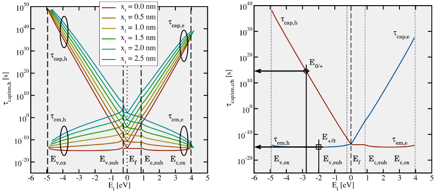
 ,
,  ). The increase in the time constants
is related to a larger tunneling distance for deeper traps. However, this effect,
incorporated in the WKB factor, becomes weaker for energies closer to the oxide
band edges since the tunneling barrier is dramatically lowered there.
). The increase in the time constants
is related to a larger tunneling distance for deeper traps. However, this effect,
incorporated in the WKB factor, becomes weaker for energies closer to the oxide
band edges since the tunneling barrier is dramatically lowered there.  ,
,  ) for the case when the Fermi
level is situated above both trap levels
) for the case when the Fermi
level is situated above both trap levels  and
and  . Since
  exceeds
 , hole capture is overcompensated by hole emission and thus effectively
suppressed.
, hole capture is overcompensated by hole emission and thus effectively
suppressed.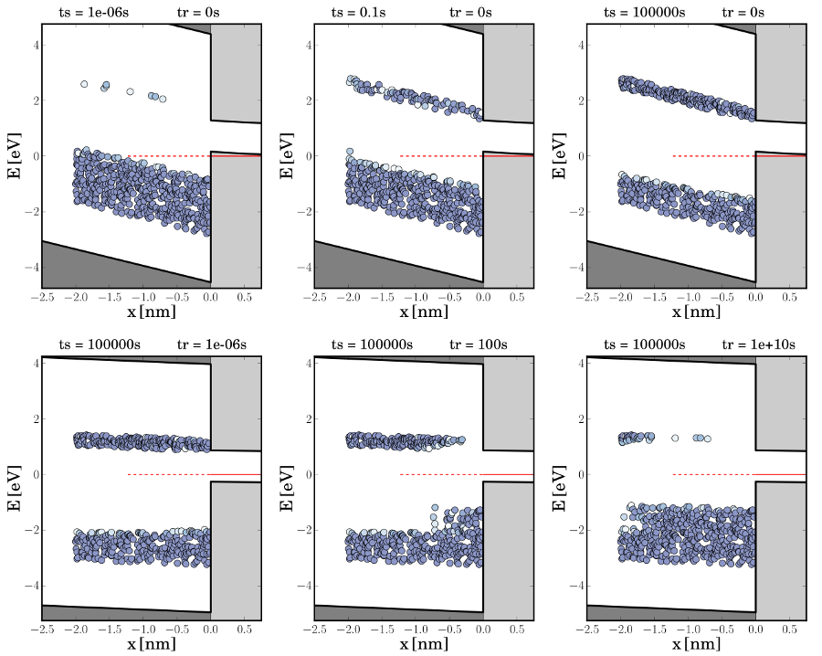
 ,
,  ). The
substrate Fermi level is indicated by the red line and the small circles represent
the trap levels
). The
substrate Fermi level is indicated by the red line and the small circles represent
the trap levels  and
and  of the single defects. The neutral defects are
assumed to have fully occupied defect orbitals and thus can only trap holes.
Therefore, they feature hole capture levels
of the single defects. The neutral defects are
assumed to have fully occupied defect orbitals and thus can only trap holes.
Therefore, they feature hole capture levels  , which are located below
the center of the substrate bandgap and are said to be ‘active’. By contrast,
the positively charged defects are assumed to be able to trap electrons only.
Accordingly, they have only electron capture levels
, which are located below
the center of the substrate bandgap and are said to be ‘active’. By contrast,
the positively charged defects are assumed to be able to trap electrons only.
Accordingly, they have only electron capture levels  above midgap but no
energy levels
above midgap but no
energy levels  , which reappear once these defects are charged again. It is
emphasized that the occupancy of one defect is related to which of its trap levels
, which reappear once these defects are charged again. It is
emphasized that the occupancy of one defect is related to which of its trap levels
 and
and  is active at the moment. Therefore, the above figures also
reflects the trap occupancies at a certain time. Since the trap levels are recorded
at the beginning, the middle, and the end of the stress and the relaxation phase,
these figures show the tunneling hole front, which is illustrated by the active
trap levels and thus the occupancy of the defects.
is active at the moment. Therefore, the above figures also
reflects the trap occupancies at a certain time. Since the trap levels are recorded
at the beginning, the middle, and the end of the stress and the relaxation phase,
these figures show the tunneling hole front, which is illustrated by the active
trap levels and thus the occupancy of the defects.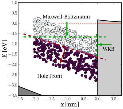
 . The capture
time constants are determined by the exponential decay in the WKB factor
and the Fermi-Dirac distribution. The latter has been approximated by the
Maxwell-Boltzmann distribution and shows an exponential energy dependence
a few
. The capture
time constants are determined by the exponential decay in the WKB factor
and the Fermi-Dirac distribution. The latter has been approximated by the
Maxwell-Boltzmann distribution and shows an exponential energy dependence
a few  away from the Fermi level. As indicated by the green vertical arrow,
this dependence leads to a tunneling hole front moving downwards in the band
diagram. By contrast, the WKB factor is most strongly affected by the trap
depth, resulting in an tunneling hole from the substrate to deep into the oxide
(green horizontal arrow). The resulting motion of the tunneling hole front is
depicted by red arrow.
away from the Fermi level. As indicated by the green vertical arrow,
this dependence leads to a tunneling hole front moving downwards in the band
diagram. By contrast, the WKB factor is most strongly affected by the trap
depth, resulting in an tunneling hole from the substrate to deep into the oxide
(green horizontal arrow). The resulting motion of the tunneling hole front is
depicted by red arrow.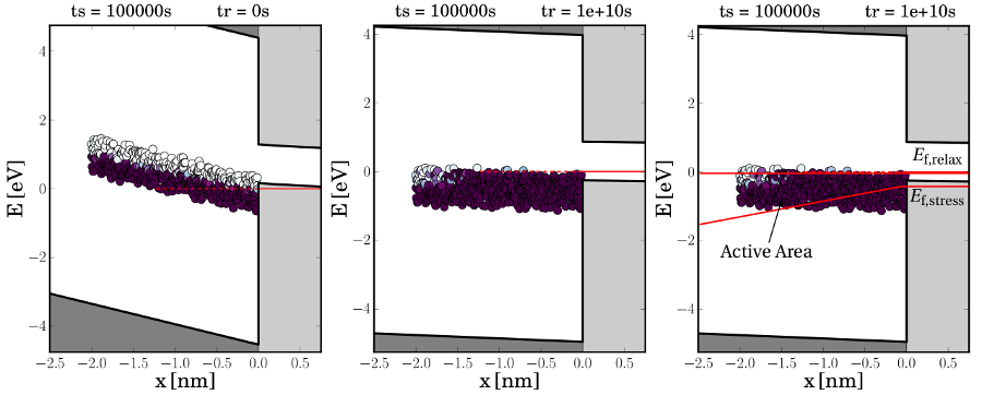
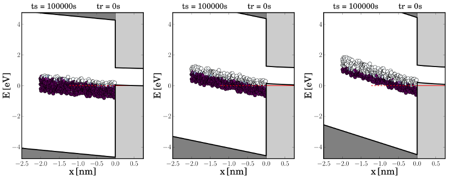
 at the end of the stress phase
for the defects shown in Fig.
at the end of the stress phase
for the defects shown in Fig.  ,
,  ). The white
circles represent neutral defects which have not trapped a hole during the stress
phase. The purple filling color indicates that the defect is positively charged
due to a finished hole capture event. Since there exist neutral defects with an
). The white
circles represent neutral defects which have not trapped a hole during the stress
phase. The purple filling color indicates that the defect is positively charged
due to a finished hole capture event. Since there exist neutral defects with an
 level above
  , hole trapping has not reached saturation after a stress
period lasting
, hole trapping has not reached saturation after a stress
period lasting  .
.  .
.  ) and relaxation (
 ). The defects situated
below
). The defects situated
below  cannot capture a hole during stress while those located above
 remain positively charged during relaxation and thus do not contribute
to
remain positively charged during relaxation and thus do not contribute
to  .
.
 as a function of stress time
for different gate biases.
as a function of stress time
for different gate biases. 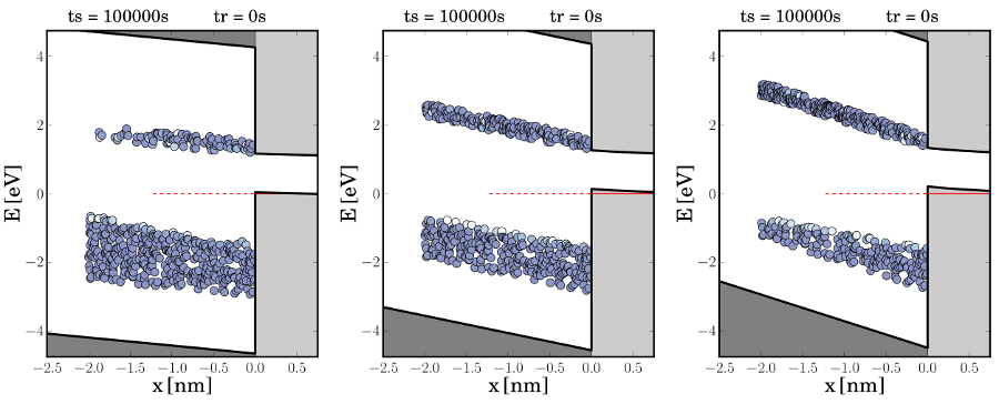
 and
and  (both second row) after a
stress time of
(both second row) after a
stress time of  for
for  (from left to right) and
 . The higher position of the
  levels goes hand in hand with
shorter hole capture times and in consequence a larger amount of trapped
charges after a stress time of
levels goes hand in hand with
shorter hole capture times and in consequence a larger amount of trapped
charges after a stress time of  . From this it can be concluded that the oxide
field dependence of the LSM primarily originates from the upwards shift of the
trap levels but is only marginally influenced by the reduced tunneling barrier
at higher
. From this it can be concluded that the oxide
field dependence of the LSM primarily originates from the upwards shift of the
trap levels but is only marginally influenced by the reduced tunneling barrier
at higher  .
.
 after a stress time
of
after a stress time
of  for
for  (from left to right) and
  . It
can be recognized that a higher
. It
can be recognized that a higher  increases the portion of
  levels above
 and thus a larger number of traps are available for hole capture.
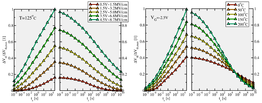
 ) when smaller biases are applied to the gate. The
degradation curves follow a nearly logarithmic behavior over a wide time range,
where the curves obtained for a small stress voltages can be better approximated
by a power-law. Furthermore, none of the curves show a sign of saturation until
a stress time of
) when smaller biases are applied to the gate. The
degradation curves follow a nearly logarithmic behavior over a wide time range,
where the curves obtained for a small stress voltages can be better approximated
by a power-law. Furthermore, none of the curves show a sign of saturation until
a stress time of  . It is noted that their slopes appear to be insensitive
to the applied gate bias — except from small gate biases again. Regarding
the relaxation phase, deviations from the time logarithmic behavior can be
recognized below
. It is noted that their slopes appear to be insensitive
to the applied gate bias — except from small gate biases again. Regarding
the relaxation phase, deviations from the time logarithmic behavior can be
recognized below  .
. 
 and
and
 demonstrate that the LSM does not reproduce the quadratic field and
temperature dependence seen in experiments.
demonstrate that the LSM does not reproduce the quadratic field and
temperature dependence seen in experiments.