9.1 Inverse Modeling
In order to be able to verify the NMP model for the experimental results,
inverse modeling is necessary. This is done via  -characteristics
of the real device. Unfortunately, the doping profile of the completely
processed pMOSFET was not accessible. To incorporate the quite
complex NMP model a representative 1D doping profile has to be
guessed .
Since the background doping is small and all the layers below the interface of the
pMOSFET are not additionally doped during the fabrication process, diffusion
from the source/drain regions towards the SiGe quantum well can take place.
Due to many annealing steps the resulting doping becomes complicated which
makes the calibration of the simulated layer structure with the proper layer
thicknesses and their corresponding dopings an extremely challenging
task.
-characteristics
of the real device. Unfortunately, the doping profile of the completely
processed pMOSFET was not accessible. To incorporate the quite
complex NMP model a representative 1D doping profile has to be
guessed .
Since the background doping is small and all the layers below the interface of the
pMOSFET are not additionally doped during the fabrication process, diffusion
from the source/drain regions towards the SiGe quantum well can take place.
Due to many annealing steps the resulting doping becomes complicated which
makes the calibration of the simulated layer structure with the proper layer
thicknesses and their corresponding dopings an extremely challenging
task.
Due to the fact that only a very limited amount of mobility data for
SiGe-layers was published so far the mobilities are only roughly approximated
and are furthermore considered as constant within the single layers. Based on the
measured mobilities of Si and Ge in [166, 167, 168, 89], the values for the layers
were linearly interpolated for  . The used values of
  are given in
Tab. 9.1 for all layers at a temperature of
are given in
Tab. 9.1 for all layers at a temperature of  .
.
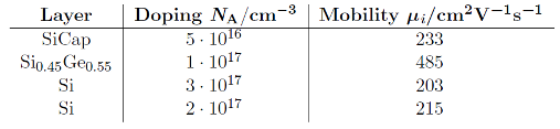
Table 9.1: Details of the used dopings inside the single layers. Based on
available measurement data the hole drift mobility was approximated.
Despite this approximation the finally obtained  -characteristics of the
1D device catches the trend of the measurement, cf. Fig. 9.2, and fits the
experimental split-
-characteristics of the
1D device catches the trend of the measurement, cf. Fig. 9.2, and fits the
experimental split- very well in the inversion regime. The decrease of the
capacitance above
very well in the inversion regime. The decrease of the
capacitance above  is due to dominant gate leakage. Below
  the gate dielectric starts to break down due to the low effective oxide thickness of
about
the gate dielectric starts to break down due to the low effective oxide thickness of
about  . Since the NBTI stress conditions dealt with in this chapter are well
within this regime, the deviations outside this regime are assumed to be
unimportant.
. Since the NBTI stress conditions dealt with in this chapter are well
within this regime, the deviations outside this regime are assumed to be
unimportant.
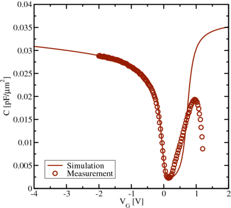
 -characteristic the layer structure can be modeled
in 1D. The simulation fits the experimental data very well in the inversion
regime, which is required during NBTI. The decrease of the capacitance
above
-characteristic the layer structure can be modeled
in 1D. The simulation fits the experimental data very well in the inversion
regime, which is required during NBTI. The decrease of the capacitance
above  is due to high gate leakage.