9.2.2 Reservoir of Holes - Classical vs. Quantum Mechanical Description
Previously [111], the holes were assumed to be energetically located at the
valence band edge of the substrate with the defects being filled corresponding to
this energy level. Unfortunately this approximation is questionable for a more
complex structure like pMOSFETs with a high-k dielectric layer and a SiGe-layer
inside the silicon substrate. This necessitates the incorporation of quantum
mechanical (QM) confinement. Instead of assuming all holes to be fixed at  ,
it is now distinguished between the contributing subbands, i.e. their different
eigenenergies and hole occupancies are considered. To obtain the wave functions
of the subbands in the channel of the MOSFET, the Schr¨odinger and Poisson
equation were solved self-consistently using the Vienna Schr¨odinger Poisson
solver (VSP2) [171]. The carrier concentration is calculated by treating the
quasi-bound states as a two-dimensional electron gas in equilibrium and the
continuum states as a 3D electron gas. The three X valley sorts of the conduction
band as well as the heavy hole, light hole, and split off band are taken into
account.
,
it is now distinguished between the contributing subbands, i.e. their different
eigenenergies and hole occupancies are considered. To obtain the wave functions
of the subbands in the channel of the MOSFET, the Schr¨odinger and Poisson
equation were solved self-consistently using the Vienna Schr¨odinger Poisson
solver (VSP2) [171]. The carrier concentration is calculated by treating the
quasi-bound states as a two-dimensional electron gas in equilibrium and the
continuum states as a 3D electron gas. The three X valley sorts of the conduction
band as well as the heavy hole, light hole, and split off band are taken into
account.
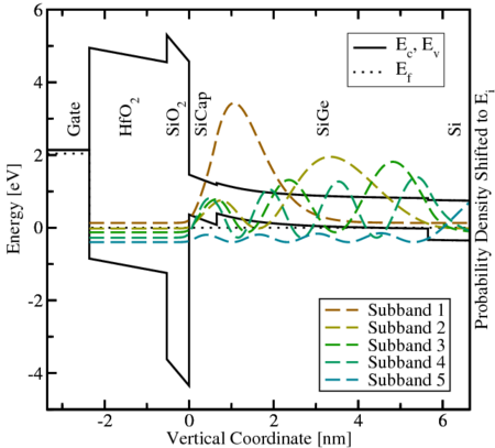
In Fig. 9.7 the first five subbands are displayed based on their corresponding
eigenenergies of which four are localized in the SiGe-layer. In Fig. 9.8 the first
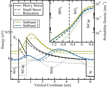
two subbands are depicted for two stress and relaxation conditions. When
switching from relaxation to stress the maxima of the subband wave functions
move towards the interface, which raises the “hole concentration” in the oxide.
The penetration of the wave functions is plotted on a log-scale to show the
transmission probability. It can be clearly seen that the contribution of the
subbands decreases with increasing order. As the bandbending inside the oxide
due to the charged defects can be neglected, the WKB approximation is valid
here and closely matches the transition probability of the wave function. Due to
the lower computational efforts, the WKB approach is therefore used in the
following.
In order to calculate the occupancy of the entire defect band during a certain
bias condition in time, the effective rates in (9.5) and (9.6) have to be evaluated
for each subband for each individual defect. The effective rates of a single defect
have then to be summed up over all subbands and determine the single defect
occupancy. The occupancy of the entire defect band finally gives the observable
degradation.