The angle between the wafer surface normal and the ion beam is the tilt angle. A non zero tilt angle is used to avoid channeling effects in crystalline silicon, to introduce dopants into the sidewalls of a trench or to implant dopants underneath a mask edge by large tilt angel implants like large tilt angle implanted drain (LATID) or large tilt angle implanted punch-through stopper (LATIPS).
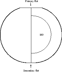
Additionally the twist angle is necessary to completely describe the direction of
incidence of the ion beam. It is the angle between the plane containing the ion
beam and the wafer normal, and the plane perpendicular to the primary flat of
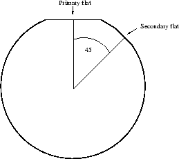
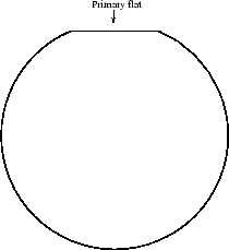
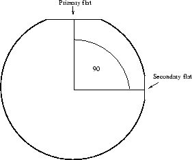
the wafer containing the wafer normal (Fig. 2.11). The primary flat
defines the orientation of the silicon crystal. It is aligned to a [011]
direction in a ![]() 100
100![]() oriented wafer. Besides the primary flat a secondary
flat is used to definitely identify a wafer type, differing by crystal
orientation and background doping (Fig. 2.12).
oriented wafer. Besides the primary flat a secondary
flat is used to definitely identify a wafer type, differing by crystal
orientation and background doping (Fig. 2.12).
|
![]()
![]()
![]()
![]() Previous: 2.2.3 Implantation Dose
Up: 2.2 Ion Implantation Process
Next: 2.3 Target Materials Properties
Previous: 2.2.3 Implantation Dose
Up: 2.2 Ion Implantation Process
Next: 2.3 Target Materials Properties