Next: 2.4.2 Deposition of SiO Up: 2.4 Material Deposition Previous: 2.4 Material Deposition Contents
One of the most effective methods to deposit material in microelectronics is to use a chemical reaction at the surface and of the underlying materials by reactant diffusion into the target material. This method is called chemical vapor deposition (CVD) and requires the underlying materials to act as catalytic materials. If a material does not, that material should at least do not react with the deposited material. However, some materials do not provide one of these mandatory requirements and therefore demand an additional barrier or seed layer, which provides the needed properties to both material layers.
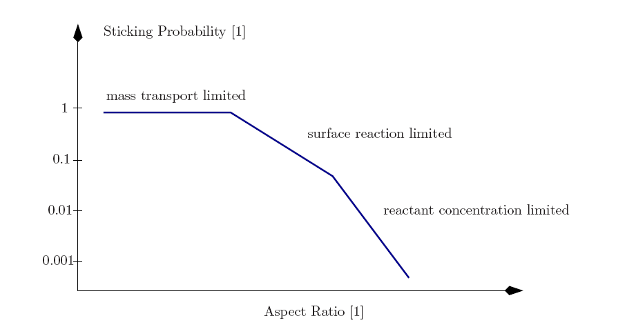
The type of the deposition can be classified into three major categories: a mass transport limited regime, a surface reaction limited regime, and a reactant concentration limited regime. As Figure 2.14 and Figure 2.15 depict, the mass transport and the surface reaction are influenced by the temperature, where all three limitations depend on the geometry. These regimes have different constraining factors which reduce the maximum deposition rate and thus the growth rate of the material in the reactor [127,25,165].
Once the materials are deposited, the possibilities to change the microstructure
of the material are very limited because the internal material structure has
mainly been defined by the deposition process.
However, there are different methods, e.g. rapid thermal annealing
(RTA) [127], dopant implantations [166,167],
and mechanical and chemical methods like CMP (chemo-mechanical
polishing) [168,169,170], which can slightly modify the microstructure.
However, all these a-posteriori methods affect the regions at the surface or a
limited region underneath the surface of the material only. For instance, if the
![]() surface is oxidized by O
surface is oxidized by O![]() or H
or H![]() O to obtain
O to obtain
![]() , the
corresponding chemical reactions use
, the
corresponding chemical reactions use
![]() from the surface. Therefore, the
thickness of the
from the surface. Therefore, the
thickness of the
![]() layer is reduced, which is often not desired for certain
applications [25].
Hence, for this case, the material has to come from an external gas source to
preserve the previous deposited layers. However, these chemical reactions follow
mostly complex pyrolytically reactions and produce a lot of highly
reactive byproducts [171].
layer is reduced, which is often not desired for certain
applications [25].
Hence, for this case, the material has to come from an external gas source to
preserve the previous deposited layers. However, these chemical reactions follow
mostly complex pyrolytically reactions and produce a lot of highly
reactive byproducts [171].
Huge efforts have been made to describe the result of the material
deposition in advance. However, due to the different and highly complex chemical
reactions inside a reactor, the predictability is still limited.
Several approaches have been proposed to deal with these problems.
There are two main approaches for the simulation of material
deposition. One approach is cell-based [167,172] and has
been introduced to describe etching of
![]() and the deposition of Tungsten and
Silicon [172]. For the
and the deposition of Tungsten and
Silicon [172]. For the
![]() deposition, a CVD process of Silan has been
considered in [173,172]. Since the description for two and
three-dimensional structures increases in complexity and memory consumption, a
level-set approach has been proposed as a second approach [174,175],
which is presented in Chapter 5.
deposition, a CVD process of Silan has been
considered in [173,172]. Since the description for two and
three-dimensional structures increases in complexity and memory consumption, a
level-set approach has been proposed as a second approach [174,175],
which is presented in Chapter 5.