Next: 3.2 Electrical Permittivity Up: 3. Thermal Models Previous: 3. Thermal Models Contents
The standard models for the electrical conductivity have been presented in Section 2.4. These models give very good results for bulk materials, where a single-crystal like behavior or an averaged material behavior can be assumed over the simulation domain. If thin film materials are considered, however, the previously presented description of bulk properties often lacks accuracy especially if the models should cover high-temperature effects. Therefore, additional material models have to be developed, which are able to describe the physics more fundamentally. Such models are intended to be implemented in simulation tools to improve the predictability of material models.
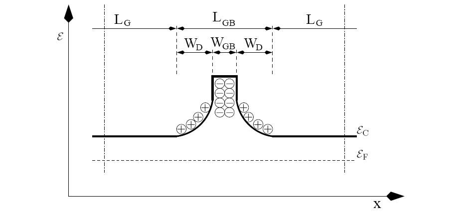
Applying single-crystal material models for bulk-sized materials chunks might can also suit well for semiconductor materials, if the internal microstructure can be neglected. However, if an additional impurity concentration can observed, a significant amount of extra energy barriers are built, as shown in Figure 3.1. Looking at the polycrystalline structure with a broader view the shape of the energy band looks more like Figure 2.12, where the typical ratio of the grain region and the grain boundaries is depicted. Here, the grains are separated by an energetic barrier consisting mostly of mismatched atoms that are located with a certain offset to the optimal lattice sites of an ideal crystal. Due to the diffusion and the segregation tendency of the impurities in the semiconductor materials, these impurity atoms move towards the interfaces of the grains and build structures as shown in Figure 3.1 at grain boundaries and at the surfaces.
To account for this type of behavior, the polycrystalline structure has been considered for contacts in transistors where additional barriers occur besides the work-function difference [177,178]. This model can be applied to other material parts where polycrystalline Si appears, for instance in contacts [177]. Consequently, a model has been developed by MANDURAH and others, which accounts for these energetic barriers so as to derive a macroscopic model that can be calibrated if the necessary information is provided by measurements (cf. (3.3) and [179,180,181,177,178]). Based on this model NATHAN and BALTES propose in [79] to use the assumptions of MANDURAH from [179,180] and extend the grain boundary model by including an average-sized grain to obtain a more reasonable conductivity model.
Applications for such models include solar cells, polycrystalline diodes for temperature measurements, fuses, and sensors in general. The advantage of this model is to predict the behavior of the polycrystalline semiconductor materials in regions where single crystal growth cannot be provided. In this case, the electrical behavior is different from devices built from single-crystal materials. For instance, the electrical resistivity highly depends on the temperature and thus also on the reverse current of a diode made of polycrystalline Si.
 |
Yet this expansion has its limits. For applications where this second-order
temperature coefficient model is not sufficiently accurate, the microscopic
structure of the material has to be included into the conductivity model.
Especially if material compounds are considered, e.g. polycrystalline silicon with high
doping for a better conduction, or silicided metals (
![]() ,
,
![]() ), the
thermal impact on the conductivity can no longer be described by these
polynomial functions. With inclusion of the microstructure into the electrical
models, the accuracy of the models can be increased.
As proposed in [79], a conductivity model which accounts for grain
boundaries [179,180,177] is combined with the drift
diffusion model for the plain grains.
), the
thermal impact on the conductivity can no longer be described by these
polynomial functions. With inclusion of the microstructure into the electrical
models, the accuracy of the models can be increased.
As proposed in [79], a conductivity model which accounts for grain
boundaries [179,180,177] is combined with the drift
diffusion model for the plain grains.
The grain boundary model for the electrical conductivity
![]() considers a ballistic transport over the barriers which can be described by the
doping concentration
considers a ballistic transport over the barriers which can be described by the
doping concentration ![]() , the interface trap density
, the interface trap density
![]() , and by the
temperature
, and by the
temperature ![]() . The other parameters are more or less constants for a certain
process technology.
Following [179,180], the model for the grain boundary
conductivity reads
. The other parameters are more or less constants for a certain
process technology.
Following [179,180], the model for the grain boundary
conductivity reads
 |
(3.4) | ||
 |
(3.5) |
To determine the global conductivity ![]() of a polycrystalline material,
NATHAN and BALTES [79] used the
MATTHIESSEN rule to combine the electrical conductivities of the grain region
of a polycrystalline material,
NATHAN and BALTES [79] used the
MATTHIESSEN rule to combine the electrical conductivities of the grain region
![]() obtained from (2.14) and (2.15) and
the grain boundary region
obtained from (2.14) and (2.15) and
the grain boundary region
![]() as
as
| (3.7) |
| (3.8) |
![$\displaystyle \sigma_{\mathrm{GB}} {=}\frac{q^2 L_{\mathrm{GB}} N \mathrm{e...
...hrm{B}}}T N W_{\mathrm{GB}}}{N_{\mathrm{t}} + N W_{\mathrm{GB}}} \right],$](img544.png)