 |
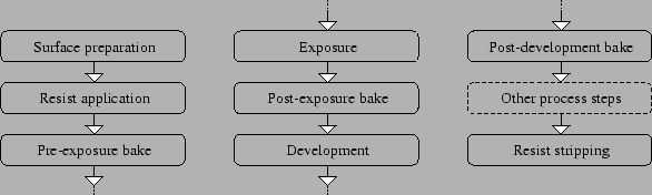
Surface preparation. Prior to resist application, the wafer surface must be cleaned, dehydrated, and primed to improve adhesion between resist and substrate. Cleaning steps are required because of the inevitable contamination which occurs during storage and handling between processing steps. As the minimum feature size is reduced particles with diameters down to 10 nm and less have to be detected. Depending on the expected contamination type and level, even chemical or dry cleaning will be required. Once the wafer surface is cleaned, a dehydration bake is performed at about 150-200 oC for 30-60 minutes to evaporate most of the absorbed water. At these temperatures typically one monolayer of water remains. The water film is strongly bonded to the surface silicon atoms in the form of silanol groups (SiOH) but does not adhere adequately to the resist. Hence, adhesion promoters are necessary to act as primers that break up the silanol groups. The OH molecule is replaced by an organic radical adhering well to the resist. The most common primer is hexamethyldisilazane (HMDS) that can either be applied in vapor or liquid form.
Resist application.
The most common method of resist application is spin coating. A
predetermined amount of resist is dispensed either on the motionless or
slowly rotating wafer. Then the wafer is rapidly accelerated up to
a maximum rotational speed ranging between 2000-6000 rpm. The
acceleration stage is crucial to obtain good uniformity since the
solvents begin evaporating from the resist immediately after dispensing.
After approximately 30 s spinning time, less than 1% of the
originally dispensed amount of the resist remains on the wafer since the rest
flies off during spinning. Typical resist thickness ranges from
0.5-1.5 ![]() m and may not vary by more than
m and may not vary by more than
![]() 5 nm (0.5%) across a flat wafer and
5 nm (0.5%) across a flat wafer and
![]() 10 nm from wafer to wafer. At this stage, the resist has
a tacky consistency since less than one third of the solvent remains.
10 nm from wafer to wafer. At this stage, the resist has
a tacky consistency since less than one third of the solvent remains.
Pre-exposure bake. After coating, the wafers must undergo a softbake or prebake to remove the resist solvent, to increase the adhesion to the wafer, and to establish the exposure characteristic. In the final photoresist the dissolution rate in the developer is highly dependent on the solvent concentration. Roughly 5% of the original solvent remains in the resist after the softbake. Typical softbake temperatures are 70-100 oC and times range from 30 s on a hotplate to 30 minutes in an oven.
Exposure. The exposure step has already been described in detail in the preceding sections. Stringent control of exposure energy is required to match the sensitivity of the photoresist (cf. Figure 2.7).
Post-exposure bake. For DQN resists the post-exposure bake is an optional step to reduce a vertically non-uniform exposure pattern caused by standing waves. A bake at 100-110 oC causes the PAC to diffuse and thereby smoothes variations in the development rate. For chemically amplified resists the post-exposure bake is required to thermally induce a chemical reaction that generates an amplified latent image (cf. Section 2.6.4).
Development. The resist development is the most critical step in photoresist processing as it plays the key role in defining the profile shape and controlling the linewidth. Nearly all positive DQN resists use alkaline developers. Common techniques are spin, spray and puddle development. In spin development, the developer is dispensed onto the rotating wafer, using the same principle as spin coating but at a much lower rotation velocity of approximately 250 rpm. Following development, the wafers are rinsed in de-ionized water to remove the remaining developer, and then dried while spinning. Spray development uses a nozzle to create a fine mist of developer over the wafer. This method reduces the required amount of developer and results in a more uniform distribution. Puddle development is the most widely used method. In this technique, the developer is slowly puddled onto the wafer surface, where it remains during the development cycle for typically 20-60 s. Independent of the used technique two important points have to be considered. Firstly, the developer has to be constantly replenished to maintain a consistent and reproducible process. Secondly, the temperature has to be controlled carefully because--like many chemical reactions--the development process is very temperature sensitive. Temperature changes of 1 oC can spoil the whole resist process.
Post-development bake. A post-development bake is often required to harden the resist against subsequent energetic processes such as ion implantation and plasma etching. Positive DQN resists are baked at 120-140 oC, whereby the resin polymer crosslinks increasing the thermal stability of the resist. Higher temperatures may cause the resist to reflow. At certain situations a reflow might be desired to produce a shallow profile so that during a subsequent etching step the sloped angle can be reproduced in the underlying film. Because of the high absorption of DUV light, resist hardening can also be achieved by exposing the resist to DUV. Crosslinking of the novolac in a thin film on the resist surface is enhanced and increases the thermal stability to approximately 200 oC.
Resist Strip. Once the resist pattern has protected the wafer during the desired sequence of process steps, e.g., ion implantation, etching or deposition, it has to be stripped from the surface. Wet-stripping of positive resists uses an organic, acid-based solution. The resist removal depends, however, on the nature of the underlying film, and on the process to which the resist pattern has been exposed. For example, a resist which has served as an ion implantation mask is usually very difficult, if not impossible, to remove by wet-stripping. Even without exposing the resist to harsh environment, wet-stripping does not always remove the resist completely, and a plasma-assisted ``descum'' becomes necessary to clean up a finally sticking monolayer of resist molecules. The most common method to complete resist removal is ``plasma ashing.'' An oxygen plasma reacts readily with the organic resist but leaves inorganic films like oxide, nitride, polysilicon, or metal mostly intact. Potential problems with plasma ashing may arise from radiation damage and charging of underlying devices.