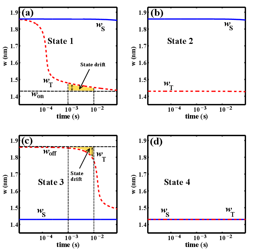
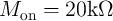
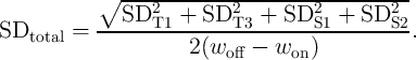
| Figure 3.6.: | Modulation of  and and  during the logic operation for different input patterns. during the logic operation for different input patterns. |
In order to analyze the TiO -based memristive circuit (Fig. 3.2), the nonlinear model is used for each
TiO
-based memristive circuit (Fig. 3.2), the nonlinear model is used for each
TiO memristive switch and thus, coupled with the equation Eq. 3.4, Eq. 3.13–Eq. 3.22 are numerically
solved for both
memristive switch and thus, coupled with the equation Eq. 3.4, Eq. 3.13–Eq. 3.22 are numerically
solved for both  and
and  . Fig. 3.6 shows the modulation of the tunnel barrier widths
  and
and  during
the implication operation for all possible input patterns (State 1–State 4) described in Table 3.2. It
illustrates that for pulse durations between 1–10 ms, only in State 1, the target memristor (T) is switched
and in all other cases both
during
the implication operation for all possible input patterns (State 1–State 4) described in Table 3.2. It
illustrates that for pulse durations between 1–10 ms, only in State 1, the target memristor (T) is switched
and in all other cases both  and
and  are left unchanged. Accordingly, correct logic behavior is achieved for
all input states and the logic result is stored as the final resistance state of
are left unchanged. Accordingly, correct logic behavior is achieved for
all input states and the logic result is stored as the final resistance state of  . Here, the initial tunnel
barriers are
. Here, the initial tunnel
barriers are 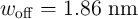 and
and 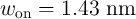 which are equivalent to
 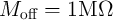 and
and
 at the readout voltage of 0.2 V (Fig. 3.4). The circuit parameters
 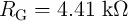 ,
,
 , and
, and 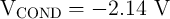 are optimized to minimize the SDE as is explained
below.
are optimized to minimize the SDE as is explained
below.
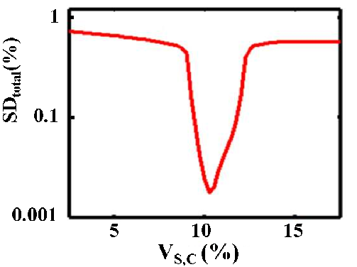
According to Fig. 3.6, the dominant SDs occur in State 1 (Fig. 3.6a) in  (
( ) and in
State 3 (Fig. 3.6c) in
) and in
State 3 (Fig. 3.6c) in  (
( ). Therefore, maximizing the modulation of the voltage
  between State 3 and State 1 (
 ) minimizes the possible SDEs in
  . Fig. 3.7 shows
 as a function of
  for different values of
  where
where
 | (3.23) |
As follows from Fig. 3.7, the optimum  corresponds to the maximum
  which maximizes the
modulation of the voltage drop on
which maximizes the
modulation of the voltage drop on  between State 3 and State 1 and thus minimizes the SDEs in
  shown in Fig. 3.6. Therefore, it is uniquely defined by the memristor’s properties,
  and
and  . By
using Fig. 3.7, an optimum
. By
using Fig. 3.7, an optimum  is obtained for each value of
  and then one can optimize
  to
minimize the gate error (Fig. 3.8).
to
minimize the gate error (Fig. 3.8).
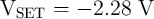
In fact, the voltage modulation  increases with increased
  and minimizes the SD in memristor
 . However, an increase in
  results in an increasing error on memristor S, because it tends to
switch
results in an increasing error on memristor S, because it tends to
switch  in State 1 (
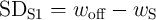 ) and State 2 (
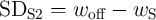 ). Therefore, there is
an optimum
). Therefore, there is
an optimum  for which the total state drift (
 ) defined as normalized root mean
square error as shown in Fig. 3.8. Optimum
) defined as normalized root mean
square error as shown in Fig. 3.8. Optimum  and
and  are determined at any
  by
by
 | (3.24) |
TiO memristive switches enable stateful implication logic by serving simultaneously as non-volatile
memory and logic gates. Although the digital data is stored in the high- and low-resistance state of the
memristive device, the internal state variable
memristive switches enable stateful implication logic by serving simultaneously as non-volatile
memory and logic gates. Although the digital data is stored in the high- and low-resistance state of the
memristive device, the internal state variable  shows analog behavior (Fig. 3.6). Therefore, during the
logic operations the voltage drops on
shows analog behavior (Fig. 3.6). Therefore, during the
logic operations the voltage drops on  and
and  tend to push
  toward
  , also when their switching is
undesired. This causes the state drift error, which accumulates in sequential logic steps and results in a
one-bit error after a certain number of implication operations. Thus, refreshing circuitry is required to
avoid this error [162]. Fig. 3.9 shows the cumulative SD in
, also when their switching is
undesired. This causes the state drift error, which accumulates in sequential logic steps and results in a
one-bit error after a certain number of implication operations. Thus, refreshing circuitry is required to
avoid this error [162]. Fig. 3.9 shows the cumulative SD in  during 20 implication operations
with 1 ms pulse duration when
during 20 implication operations
with 1 ms pulse duration when  and
and  are in high and low resistance states, respectively
(State 3). It illustrates that after 14 steps the sate variable
are in high and low resistance states, respectively
(State 3). It illustrates that after 14 steps the sate variable  is equal to the median value of
 1.65 nm which can be readout either as high- or low-resistance state. Whereas any
resistance switching in State 3 is considered as an undesired switching, the initial logic state of
1.65 nm which can be readout either as high- or low-resistance state. Whereas any
resistance switching in State 3 is considered as an undesired switching, the initial logic state of  has to be
rewritten before
has to be
rewritten before  reaches 1.65 nm. It is worth mentioning that the linear model predicts a
SD of 48.9% [162] for a particular design example which means a refreshing is required after
each implication operation. Compared to the nonlinear ionic drift model, the linear drift model
exhibits higher state drift values since it assumes that the state drift is directly proportional to the
current or voltage of the memristive devices. However, according to experimental data, the ionic
drift velocity shows an exponential dependence on the applied current or voltage [148] which
is taken into account in the nonlinear model by Eq. 3.20 and Eq. 3.21. Once again one has
to note that, as high switching voltages are used for (high-speed) computing, the memristor
nonlinear model has to be used to take the tunneling effect and dynamical memristor behavior into
account.
reaches 1.65 nm. It is worth mentioning that the linear model predicts a
SD of 48.9% [162] for a particular design example which means a refreshing is required after
each implication operation. Compared to the nonlinear ionic drift model, the linear drift model
exhibits higher state drift values since it assumes that the state drift is directly proportional to the
current or voltage of the memristive devices. However, according to experimental data, the ionic
drift velocity shows an exponential dependence on the applied current or voltage [148] which
is taken into account in the nonlinear model by Eq. 3.20 and Eq. 3.21. Once again one has
to note that, as high switching voltages are used for (high-speed) computing, the memristor
nonlinear model has to be used to take the tunneling effect and dynamical memristor behavior into
account.
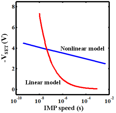
| Figure 3.10.: | Optimized  pulse amplitude as a function of the pulse duration (IMP speed) based on the linear and
the nonlinear memristor models. pulse amplitude as a function of the pulse duration (IMP speed) based on the linear and
the nonlinear memristor models. |
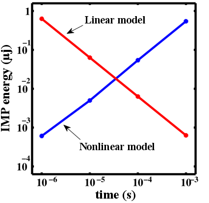
| Figure 3.11.: | Average implication operation energy ( ) as a function of the IMP speed based on the linear and the
nonlinear memristor models. ) as a function of the IMP speed based on the linear and the
nonlinear memristor models. |
Fig. 3.10 shows only a slight increase of the optimized  pulse amplitude with the implication switching
time decreased in contrast to the linear model. This results in large power consumption benefits at higher
IMP speed (Fig. 3.11) and shows a good agreement between simulations based on the nonlinear model and
the available experimental data (see Fig. S5(b) in Supplementary Information of [75]) which demonstrates a
decrease in switching energy of a TiO
pulse amplitude with the implication switching
time decreased in contrast to the linear model. This results in large power consumption benefits at higher
IMP speed (Fig. 3.11) and shows a good agreement between simulations based on the nonlinear model and
the available experimental data (see Fig. S5(b) in Supplementary Information of [75]) which demonstrates a
decrease in switching energy of a TiO memristive device with the pulse duration decreased. In fact,
Fig. 3.11 demonstrates that when the linear model is used, event the trend of the average implication
energy consumption (
memristive device with the pulse duration decreased. In fact,
Fig. 3.11 demonstrates that when the linear model is used, event the trend of the average implication
energy consumption ( ) is wrongly predicted as it shows an increase with the IMP speed
increased.
) is wrongly predicted as it shows an increase with the IMP speed
increased.
 | (3.25) |
where  denotes the implication energy consumption when the memristive devices
  and
and  are
initially in State
are
initially in State  .
.
 as a function of
  for different values of
  .
.
 .
.
 for State 3.