4.4 Reprogrammable Logic Using STT-MTJs
Recently, it has been demonstrated that by using direct communication between STT-MTJs, logic
operations can be realized for which the MTJ devices are used simultaneously as memory and
computing elements in intrinsic logic-in-memory architectures. In [54] and [55] experimental
demonstrations of two-input and three-input reprogrammable logic gates (Fig. 4.18) are reported to realize
the basic Boolean logic operations AND, OR, NAND, NOR, and the Majority operation. This
section describes the operating principle and presents a reliability analysis of the reprogrammable
gates.
The basic Boolean logic operations using reprogrammable gates are executed in two sequential steps. These
steps comprise an appropriate preset operation (parallel or antiparallel state) in the output MTJ and then
applying a voltage pulse ( ) with a proper amplitude to the gate. Depending on the logic states of the
input MTJs (
) with a proper amplitude to the gate. Depending on the logic states of the
input MTJs ( ), the preset in the output MTJ (
 ), and the voltage level applied to the gate, a
conditional switching behavior in the output MTJ is provided that corresponds to a particular logic
operation [55].
), and the voltage level applied to the gate, a
conditional switching behavior in the output MTJ is provided that corresponds to a particular logic
operation [55].
| Table 4.1.: | Realized conditional switching behavior is equivalent to the AND and OR operations with a preset of  using the two-input reprogrammable gate. Desired switching events in the output (
 ) are indicated by boldface type. ) are indicated by boldface type. |
|
|
|
|
|
|
| | |
| | |
|
| | |
|
|
|
| | |
| | | | | |
|
|
|
|
|
|
| | |
State | |  |  |  |  |  |
|
|
|
|
|
|
|
|
|
| 1 | LRS (0) | LRS (0) | HRS (1) | LRS (0) | HRS (1) | LRS (0) |
|
|
|
|
|
|
|
|
|
| 2 | LRS (0) | HRS (1) | HRS (1) | LRS (0) | HRS (1) | HRS (1) |
|
|
|
|
|
|
|
|
|
| 3 | HRS (1) | LRS (0) | HRS (1) | LRS (0) | HRS (1) | HRS (1) |
|
|
|
|
|
|
|
|
|
| 4 | HRS (1) | HRS (1) | HRS (1) | HRS (1) | HRS (1) | HRS (1) |
|
|
|
|
|
|
|
|
|
| |
Table 4.1 and Table 4.2 illustrate how the AND, OR, NAND, and NOR operations are performed employing
the two-input reprogrammable gate in two steps. The variable  show the logic states of an input
MTJ (X
show the logic states of an input
MTJ (X ) and
) and  represents the logic state of the output MTJ (Y). In order to perform a
logic operation, first a preset of
represents the logic state of the output MTJ (Y). In order to perform a
logic operation, first a preset of  (setting Y in the high-resistance state (HRS) shown
in Table 4.1) or
(setting Y in the high-resistance state (HRS) shown
in Table 4.1) or  (setting Y in the low-resistance state (LRS) shown in Table 4.2) is
performed in the output MTJ (Step 1). In Step 2 a proper voltage level (
(setting Y in the low-resistance state (LRS) shown in Table 4.2) is
performed in the output MTJ (Step 1). In Step 2 a proper voltage level ( or
or  with
optimized amplitude explained in Section 4.3.2) is applied to the gate to enforce the desired
(high-to-low or low-to-high) resistance switching event in the output MTJ to execute the logic
operation AND/OR or NAND/NOR. Compared to the (N)AND operation, the (N)OR operation
requires a lower voltage amplitude (
with
optimized amplitude explained in Section 4.3.2) is applied to the gate to enforce the desired
(high-to-low or low-to-high) resistance switching event in the output MTJ to execute the logic
operation AND/OR or NAND/NOR. Compared to the (N)AND operation, the (N)OR operation
requires a lower voltage amplitude ( ), as it must enforce a desired switching event only,
if both input MTJs are in the low resistance state (State 1). For the (N)AND operation the
switching events are enforced not only in State 1 but also when only one of the inputs is in the
low resistance state (State 2 and State 3). These switching events in State 2 and State 3 are
desired switching events for the (N)AND operation, while they are undesired events for the (N)OR
operation.
), as it must enforce a desired switching event only,
if both input MTJs are in the low resistance state (State 1). For the (N)AND operation the
switching events are enforced not only in State 1 but also when only one of the inputs is in the
low resistance state (State 2 and State 3). These switching events in State 2 and State 3 are
desired switching events for the (N)AND operation, while they are undesired events for the (N)OR
operation.
| Table 4.2.: | Realized conditional switching behavior is equivalent to the NAND and NOR operations with a preset of
 using the two-input reprogrammable gate. using the two-input reprogrammable gate. |
|
|
|
|
|
|
| | |
| | |
|
| | |
|
|
|
| | |
| | | | | |
|
|
|
|
|
|
| | |
State | |  |  |  |  |  |
|
|
|
|
|
|
|
|
|
| 1 | LRS (0) | LRS (0) | LRS (0) | HRS (1) | LRS (0) | HRS (1) |
|
|
|
|
|
|
|
|
|
| 2 | LRS (0) | HRS (1) | LRS (0) | HRS (1) | LRS (0) | LRS (0) |
|
|
|
|
|
|
|
|
|
| 3 | HRS (1) | LRS (0) | LRS (0) | HRS (1) | LRS (0) | LRS (0) |
|
|
|
|
|
|
|
|
|
| 4 | HRS (1) | HRS (1) | LRS (0) | LRS (0) | LRS (0) | LRS (0) |
|
|
|
|
|
|
|
|
|
| |
Conditional switching corresponding to specific logic operations in reprogrammable logic gates
(Fig. 4.18) are performed by applying a proper voltage  to the gates. For given MTJ device
characteristics, the value of the circuit parameter
to the gates. For given MTJ device
characteristics, the value of the circuit parameter  has to be optimized to ensure a reliable
conditional switching behavior of the output MTJ for any possible input pattern. Indeed, for any logic
operation performed by the reprogrammable gates, this optimization is required to maximize
(minimize) the switching probability in the output MTJ (
has to be optimized to ensure a reliable
conditional switching behavior of the output MTJ for any possible input pattern. Indeed, for any logic
operation performed by the reprogrammable gates, this optimization is required to maximize
(minimize) the switching probability in the output MTJ ( or
or  ), when it is a
desired (an undesired) switching event in Step 2 (Table 4.1 and Table 4.2). Therefore, for the
reliability analysis, the error probability of a given input state (State
), when it is a
desired (an undesired) switching event in Step 2 (Table 4.1 and Table 4.2). Therefore, for the
reliability analysis, the error probability of a given input state (State  ) is defined as
  (
( ) for a desired (undesired) switching event, where
  is the switching probability of
the output MTJ in State
is the switching probability of
the output MTJ in State  . It should be noted that the input MTJs are left unchanged and
thus their switching probabilities are negligible as the current flowing through the output MTJ
splits between the inputs, and their currents are below the critical current required for the STT
switching.
. It should be noted that the input MTJs are left unchanged and
thus their switching probabilities are negligible as the current flowing through the output MTJ
splits between the inputs, and their currents are below the critical current required for the STT
switching.
Similar to the implication gates (Eq. 4.21), by assuming equal incidence probabilities for all input patterns,
we obtain the average error probability ( ) of a basic logic operation
  implemented by the
reprogrammable gate as
implemented by the
reprogrammable gate as
 | (4.22) |
where  is the number of input MTJs. By using Table 4.1, Table 4.2, and Eq. 4.22,
  is obtained for the
two-input (N)OR and (N)AND operations as
is obtained for the
two-input (N)OR and (N)AND operations as
| EOR = ENOR =  ∑
i=14E
i = ∑
i=14E
i =  [(1 - P1) + P2 + P3 + P4], [(1 - P1) + P2 + P3 + P4], | (4.23)
|
| EAND = ENAND =  ∑
i=14E
i = ∑
i=14E
i =  [(1 - P1) + (1 - P2) + (1 - P3) + P4], [(1 - P1) + (1 - P2) + (1 - P3) + P4], | (4.24) |
where  is the switching probability of the output MTJ in State
  .
.
It is important to note that for the AND and OR operations  represents the probability for antiparallel to
parallel (AP–to–P) magnetization switching, while it is the probability for the P–to–AP switching in the case
of NAND and NOR operations. In order to calculate
represents the probability for antiparallel to
parallel (AP–to–P) magnetization switching, while it is the probability for the P–to–AP switching in the case
of NAND and NOR operations. In order to calculate  for different input patterns and various logic
operations, we use Eq. 4.15 which express the MTJ’s switching probability as a function of the applied
current. For calculating the current flowing through each MTJ, the voltage-dependent effective TMR model
(Eq. 4.18) is used coupled with Kirchhoff’s laws applied to the two- and three-input reprogrammable gates
(Fig. 4.18).
for different input patterns and various logic
operations, we use Eq. 4.15 which express the MTJ’s switching probability as a function of the applied
current. For calculating the current flowing through each MTJ, the voltage-dependent effective TMR model
(Eq. 4.18) is used coupled with Kirchhoff’s laws applied to the two- and three-input reprogrammable gates
(Fig. 4.18).
Fig. 4.19 shows the different values of  for the AND (left) and the NAND (right) logic operations based
on the two-input reprogrammable gate as a function of
for the AND (left) and the NAND (right) logic operations based
on the two-input reprogrammable gate as a function of  . MTJs are characterized as
  ,
,
 ,
,  , and
, and  . For a voltage level
  chosen within the reliable
gap (RG) opened between the switching windows (SWs) of the nearest desired (
chosen within the reliable
gap (RG) opened between the switching windows (SWs) of the nearest desired ( ) and undesired (
 )
switching events, the average error probability is minimized. Fig. 4.20 shows the average error probabilities
(
)
switching events, the average error probability is minimized. Fig. 4.20 shows the average error probabilities
( ) for different logic operations for the two- and three-input reprogrammable gates as a function of
  .
It illustrates that for each operation there is an optimal
.
It illustrates that for each operation there is an optimal  and for both two- and three-input
gates the operations AND and NAND offer higher reliability as compared to the other logic
operations.
and for both two- and three-input
gates the operations AND and NAND offer higher reliability as compared to the other logic
operations.
In fact, as it is shown in Table 4.1 and Table 4.2, the operations AND and NAND exhibit undesired
switching when the inputs ( and
and  ) are in high-resistance state (State 4), but a desired switching when
one of the inputs is in the low-resistance state (State 2 or State 3); and the operations OR and NOR exhibit
a desired switching when the inputs (
) are in high-resistance state (State 4), but a desired switching when
one of the inputs is in the low-resistance state (State 2 or State 3); and the operations OR and NOR exhibit
a desired switching when the inputs ( and
and  ) are in the low-resistance state (State 1) but undesired
switching when one of the inputs is in the high-resistance state (State 2 or State 3). Eq.4.25 shows that the
change in resistance at the input (
) are in the low-resistance state (State 1) but undesired
switching when one of the inputs is in the high-resistance state (State 2 or State 3). Eq.4.25 shows that the
change in resistance at the input ( ) is higher when there is a modulation between State 4
and State 2 (or State 3) rather than a modulation between State 1 and State 2 (or State 3)
(
) is higher when there is a modulation between State 4
and State 2 (or State 3) rather than a modulation between State 1 and State 2 (or State 3)
( ).
).
| |ΔRin(4, 3)|-|ΔRin(3, 1)| | =  - (Rin(3) - Rin(1)) - (Rin(3) - Rin(1)) | |
|
| =  - (Rin(2) - Rin(1)) - (Rin(2) - Rin(1)) | |
|
| =  - - | |
|
| =  > 0 > 0 | (4.25) |
It is clear that a higher resistance modulation in the input MTJs provides a higher current modulation in the
output MTJ of a reprogrammable logic gate (Fig. 4.18). As a result, according to Eq.4.25, the current
flowing through the output MTJ has a higher modulation, when State 2 (or State 3) is compared to State 4
rather than to State 1.
| |Rin(4) - Rin(2, 3)| > | |Rin(2, 3) - Rin(1)| | |
|
| ⇒ | |Iout(4) - Iout(2, 3)| > |Iout(2, 3) - Iout(1)| | (4.26) |
Therefore, the modulation between the nearest desired ( ) and undesired (
 ) switching events for the
(N)AND operation is higher than that of between the nearest desired (
) switching events for the
(N)AND operation is higher than that of between the nearest desired ( ) and undesired (
 )
events for the (N)OR operation. Thus, the (N)AND operation provide a more reliable behavior
(Fig. 4.20).
)
events for the (N)OR operation. Thus, the (N)AND operation provide a more reliable behavior
(Fig. 4.20).
The logic implementation using MTJ-based logic gates relies on a state dependent current modulations on
the output (target) MTJs. These modulations are caused by the changes in the MTJs’ resistances for
different initial logic states. According to Eq. 4.18, the resistance modulation between the high and low
resistance states in the MTJ with antiparallel and parallel magnetization alignments is proportional to the
TMR ratio of the MTJs. Therefore, from a device point of view, the average error probabilities of all
MTJ-based operations are expected to decrease with increasing TMR ratio. In fact, as we will see later, the
TMR ratio is considered as a very important device parameter for the reliability of all STT-MTJ-based logic
gates. The width of the reliable gap between the switching probabilities in the reprogrammable gate ( in
Fig. 4.19) is enlarged for a higher TMR ratio as the difference between the different input states originates
from the modulation between the HRS and the LRS of the MTJs (Table 4.1 and Table 4.2). It is also
clear that a resistance modulation (the difference between the HRS and the LRS states) of one
input MTJ causes a higher current modulation in the output MTJ, when it is only connected
(in parallel) to one other input MTJ rather than two input MTJs. Therefore, compared to the
three-input reprogrammable gate, the two-input reprogrammable gate provides a higher current
modulation in its output MTJ and thus exhibits a more reliable logic behavior (see
in
Fig. 4.19) is enlarged for a higher TMR ratio as the difference between the different input states originates
from the modulation between the HRS and the LRS of the MTJs (Table 4.1 and Table 4.2). It is also
clear that a resistance modulation (the difference between the HRS and the LRS states) of one
input MTJ causes a higher current modulation in the output MTJ, when it is only connected
(in parallel) to one other input MTJ rather than two input MTJs. Therefore, compared to the
three-input reprogrammable gate, the two-input reprogrammable gate provides a higher current
modulation in its output MTJ and thus exhibits a more reliable logic behavior (see  for different
operations in Fig. 4.20). Accordingly, in the following we employ only the two-input gate for the
performance analysis and comparison between the reprogrammable and the implication logic
architectures.
for different
operations in Fig. 4.20). Accordingly, in the following we employ only the two-input gate for the
performance analysis and comparison between the reprogrammable and the implication logic
architectures.
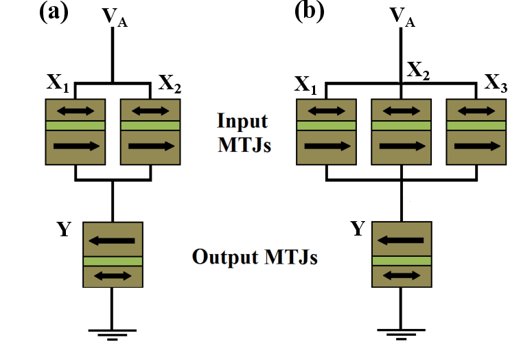
 (Y) shows an input
(output) MTJ.
(Y) shows an input
(output) MTJ.


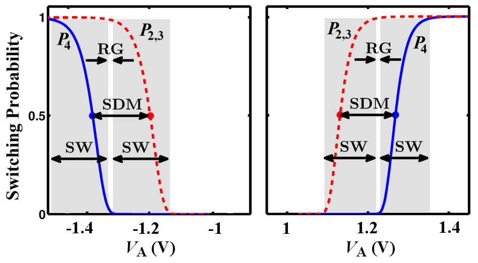
 ) and undesired (
 ) switching events shown for the
AND (left side) and NAND (right side) operations.
) switching events shown for the
AND (left side) and NAND (right side) operations.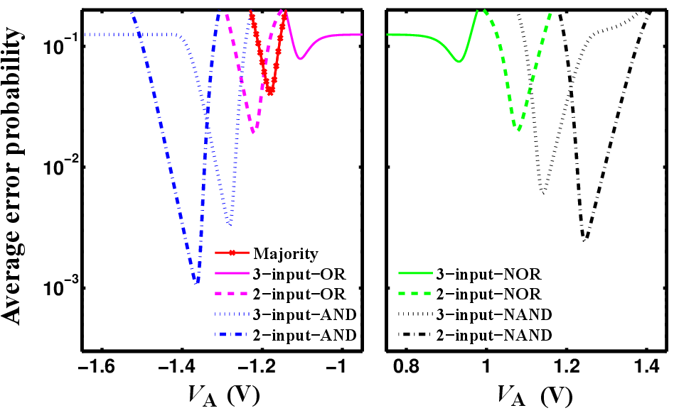
 .
.