Chapter 3
Stochastic Model of the Resistive Switching
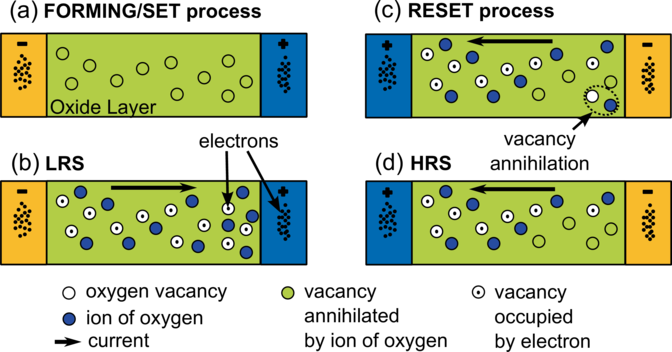
3.1 Switching Mechanism
The resistive switching behavior in the oxide-based memory is associated with the formation and rupture of a conductive
filament. The conductive filament is formed by localized oxygen vacancies V o [72] or domains of V o. The conduction is due
to electron hopping between these V o. Figure 3.1 shows schematic illustration of the resistive switching mechanism in
bipolar oxide-based memory. Formation and rupture of the conductive filament is due to a redox reaction in
the oxide layer under a voltage bias. If a positive voltage is applied, the formation of a conductive filament
begins, when the voltage reaches a critical value sufficient to create V o by moving an oxygen ion (O2-) to an
interstitial position. This leads to a sharp increase in the current signifying a transition to a state with low
resistance.
If a reverse negative voltage is applied, the current increases linearly, until the applied voltage reaches the value at which
annihilation of V o is triggered by means of moving O2- to V
o. The conductive filament is ruptured and so the current
decreases. This is the transition to a state with high resistance.
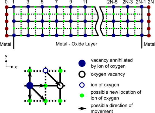
3.2 Model Systems Description
Figure 3.2 shows the unit cell of the two-dimensional (2D) model system. Columns with numbers 0 and 2N
are reserved for the electrodes (there are generators and receivers of electrons in a model system). Places in
odd-numbered columns at the intersections of the solid lines are reserved for oxygen vacancies V o. An oxygen
vacancy is formed, when an oxygen ion O2- moves to a nearest empty interstitial position located at the
intersections of the dotted lines (Figure 3.2). An oxygen vacancy can be occupied by an electron hopping
from another oxygen vacancy or from an electrode. Alternatively, an oxygen vacancy can be annihilated by
an oxygen ion O2- coming from a nearest interstitial position provided the vacancy is not occupied by an
electron.
3.3 Electron Hopping and Ion Motion
For modeling electrical conductivity in the low resistance state (i.e., when conductive filament is formed) by a Monte Carlo
technique [134],[153], the following events are allowed:
- an electron hop into V o from an electrode;
- an electron hop from V o to an electrode;
- an electron hop between two V os.
In order to model the dependences of transport on the applied voltage and temperature the hopping rates for electrons
are chosen as [224]:
 | (3.1) |
Here, ℏ is the reduced Planck constant, Ae is a dimensionless coefficient, ΔE is the difference between the energies of an
electron positioned at sites n and m, Rnm is the hopping distance, a is the localization radius, T is the temperature, kB is
the Boltzmann constant. When an external voltage U is applied, the energy difference ΔE includes the corresponding
voltage dependent term.
 | (3.2) |
Here, d is the x-dimension of system, and Δx = xm - xn is the difference between the x coordinate of the sites
(vacancies) m and n.
Rates (Equation 3.1) are similar to those used in a single-electron transport theory [153]. An exponential in the
denominator guarantees an exponentially small equilibrium occupation of a site m as compared to the occupation of a site n,
if the condition Em - En ≫ kBT is satisfied. When the opposite condition En - Em ≪ kBT is fulfilled, the rate is
proportional to the external field U∕d. Therefore, rates (Equation 3.1) can mimic an Ohmic (linear in external field)
transport in a system of equivalent sites having the same energy.
To further specify the electron dynamics, an electron is assumed to hop from the site n to the site m may occur only, if
the site n was occupied and the site m was empty before the hopping event. This is a manifestation of the fact that the
energy gap separating the vacancies with one and two electrons is assumed large enough that the double occupancy of a
vacancy becomes prohibitively small.
The hopping rates between an electrode (0 or 2N) and an oxygen vacancy m are described by [72]
 | (3.3) |
 | (3.4) |
Here, α and β are the coefficients of the boundary conditions on the cathode and anode, respectively, A and C stand for
cathode and anode, respectively, and i and o for hopping on the site and out from the site. Contrary to an
oxygen vacancy, an electrode is assumed to have enough electrons so that hopping from an electrode to a
vacancy is always allowed, provided the vacancy was empty before the event. Complimentary, an electrode
has always a place to accept a carrier, so an electron can always hop at an electrode provided this event is
allowed.
The current generated by hopping is calculated as
 | (3.5) |
Here, qe is the electron charge, t =  -1 is the time spent for moving an electron at a distance
Δx, fn = 1(0), if the site n is occupied (empty), f0 = α and f2N = β, if an electron hops from an electrode, and
(1 - f0) = α and (1 - f2N) = β, if a hop to an electrode occurs. Thus, qeΔx∕d is a charge passing through an external
circuit during a single hopping event [134]. The summation in Equation 3.5 is over all hopping events. Therefore,
Equation 3.5 gives the current as the total charge passing through the external circuit during the total time ∑
t divided by
the total time.
-1 is the time spent for moving an electron at a distance
Δx, fn = 1(0), if the site n is occupied (empty), f0 = α and f2N = β, if an electron hops from an electrode, and
(1 - f0) = α and (1 - f2N) = β, if a hop to an electrode occurs. Thus, qeΔx∕d is a charge passing through an external
circuit during a single hopping event [134]. The summation in Equation 3.5 is over all hopping events. Therefore,
Equation 3.5 gives the current as the total charge passing through the external circuit during the total time ∑
t divided by
the total time.
For modeling the resistive switching in oxide-based memory, in addition to the possible events of moving an electron, the
dynamics of oxygen ions (O2-) is introduced as follows:
- formation of V o by O2- moving to an interstitial position;
- annihilation of V o by moving O2- to V
o.
To describe the field-induced ion dynamics the ion rates are chosen similarly to Equation 3.1 as follows:
 | (3.6) |
Here it is assumed that O2- can move from the lattice site to the nearest interstitial provided the interstitial is empty.
Alternatively, O2- can move back from the interstitial to the nearest vacancy, provided it is not occupied by an electron.
Because moving an ion is allowed only at the nearest sites, a distance-dependent term is incorporated in Ai.
When the external voltage is applied, the difference in energy of an ion after and before hopping is computed
as
 | (3.7) |
Here, Ec is a threshold energy for the mth vacancy V o (Ef) or annihilation energy of the mth vacancy V o (Ea), when
O2- is moving to an interstitial or back to V
o, respectively. The values of these energies depend on the insulating
material.
3.4 Applications of Stochastic Based Method
All calculations are carried out on one or/and two-dimensional lattices, and the distances between two nearest neighboring
V o in all directions are equal, if no voltage or temperature is applied. Despite the fact that in the binary metal oxides oxygen
vacancies can have three different charge states with charges 0, +1, and +2, to simplify the model, it is assumed that the
oxygen vacancy is either empty or occupied by one electron [72]. This assumption is not a limitation, however, since, due to
an energy separation between the three charge states, only two of them will be relevant for hopping and significantly
contribute to transport.
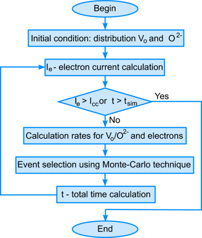
Flowchart of the microscopic simulation of the resistive switching is presented in Figure 3.3.
3.4.1 Electron motion simulation
Calculation of electron occupation probability
Following [54], hopping is only allowed in one direction and only to/from the closest V o. Each site i of a one-dimensional
lattice of N sites is either occupied by an electron or empty; during a time interval dt, each electron has a probability Γnm of
hopping to its right, provided the target site is empty; moreover, during the time interval dt, an electron may enter the
lattice at Site 1 with probability α ⋅ Γ01 (if this site is empty) and an electron at Site N may leave the lattice
with probability β ⋅ ΓN(N+1) (if this site is occupied). For calibration the exact results [54] were used. The
occupation probability of a central V o (pc) is described, depending on the boundary conditions, as follows
[54]: 1) for α > 0.5 and β > 0.5, pc = 0.5; 2) α < 0.5 and α < β, pc = α; 3) β < 0.5 and β < α, pc = 1 - β.
Figure 3.4 shows simulation results of the stochastic model, which fully coincide with theoretical calculations
[54].
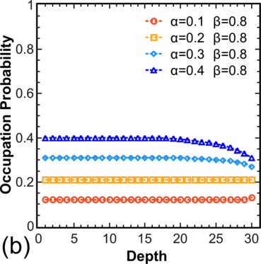
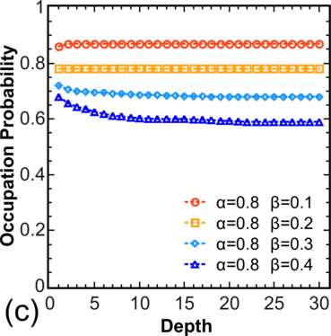
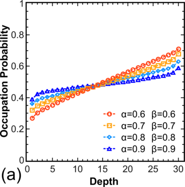
To move from the model system [54] to more realistic systems, the distribution of electron occupations for a chain is
calculated, where hopping is allowed not only to/from the nearest V o (Figure 3.5, left), and for systems with T > 0, where
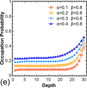
hopping is allowed in both directions (Figure 3.5, right). Note that for α > 0.5 and β > 0.5 one still has pc = 0.5
in the center, while for other values α,β one observes a decrease in pc for α < β and an increase in pc for
β < α.
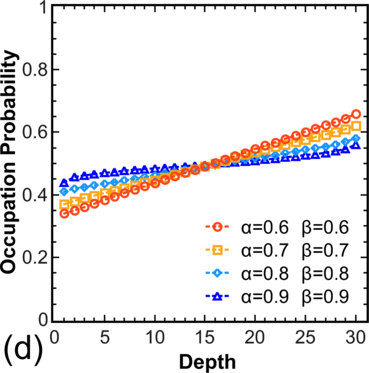
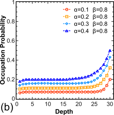
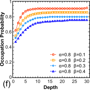
Next, the model is calibrated in a manner to reproduce the results reported in [72], for V =0.4V to V =1.6V. Figure 3.6a
shows a case, where the hopping rate between the electrodes and V o is larger than the rate between the two V o (i.e.
α,β > 1). In this case the low occupation region is formed near the anode, which according to [72] would correspond to an
unipolar behavior. Figure 3.6b shows a case, where the hopping rate between the two V o is larger than the rate between the
electrodes and V o (i.e. α,β < 1). In this case the low occupation region is formed near the cathode, which would correspond
to bipolar behavior [72].
In practice, the coefficients of the boundary conditions are determined by the material properties from which the
electrode and the oxide-layer are made. The dependence of resistive switching on the electrode material was recently
reported in research for TiO2 [130] and ZrO2 [156].
Modeling the temperature dependence
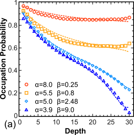
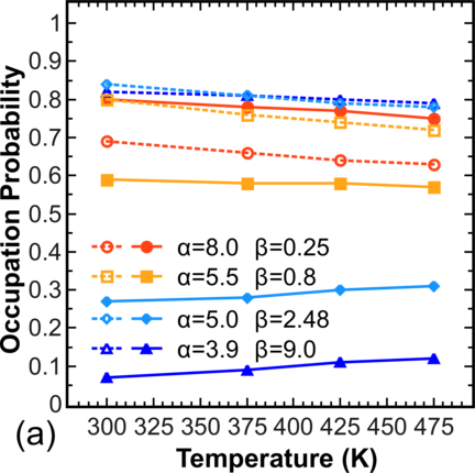
Following [72], the rupture of the conductive filament is possible only in the low electron occupation region. In order to
simulate failures in switching from a state with low resistance to a state with high resistance for an elevated temperature, the
dependence of the electron occupation distribution near the anode and the cathode for a system with α,β > 1 (Figure 3.7a)
and α,β < 1 (Figure 3.7b) was calculated. In both types of systems the change is marginal amounting to less than 10% for a
temperature increase from 300K to 475K. This result indicates high robustness of failure-free RRAM switching from a
state with low resistance to a state with high resistance for elevated temperature. At the same time it has
been found that the measured decrease of switching time with increasing temperature reported in [72] stems
from the increased mobility of oxide ions rather than from reduced occupations of V o in the low occupation
region.
3.4.2 Modeling of the SET/RESET process
Single conductive filament devices
For the simulations a one-dimensional lattice consisting of thirty equivalent, equidistantly positioned hopping sites has
been used. To simplify calculations the coefficients of the boundary conditions are assumed to be constant and equal to 0.1,
independent of the applied voltage. In both simulations (SET and RESET process) the same formation/annihilation energy
for V o was used. For simulations the ratio Ai∕Ae is equal to 10-3. The result of the simulation of the SET process is shown
in Figure 3.8.
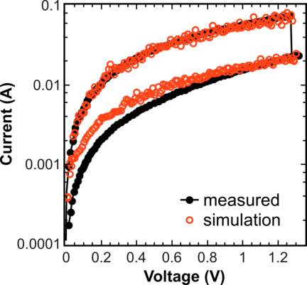
To further demonstrate the capabilities of the model, the RESET I - V characteristics for a single-CF device [72] was
also simulated. For this purpose the conductive filament was modified in such a way that for each V o an oxygen ion is placed
nearby, to provide a possibility for the vacancies to annihilate. In the first moment of time all V o are formed and assumed to
be unoccupied by electrons. Electrons can enter/leave the system and hop from/to an electrode, respectively, or
hop between two V o according to the rules described above (Equations 3.1-3.4) Each O2- has a probability
Γn′ (Equation 3.6) of annihilation with the nearest V o if this V o is not occupied by an electron. Figure 3.9
shows the simulation result of the stochastic model, which is in good agreement with measurements from
[72].
Multiple conductive filament devices
In real systems formation of several conductive filaments is possible. To allow this formation a two-dimensional lattice
(2 × 30) is used now and the process of the resistive switching by applying a voltage V with a saw-tooth like time
dependence is investigated. The coefficients of the boundary conditions are constant and taken to be equal to
0.1.
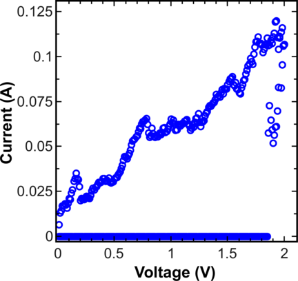
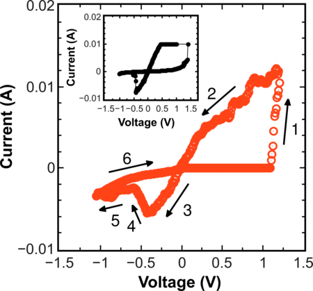
Figure 3.10 shows the I -V obtained with the model system during a full cycle of switching from HRS to LRS and back.
In the first moment of time it is assumed that there are no vacancies V o in the system. If a positive voltage is applied, the
formation of a conductive filament begins, when the voltage reaches a critical value sufficient to create V o by moving O2- to
an interstitial position. During the SET and the RESET process each O2- has a probability Γ
n′ of moving to the
nearest interstitial position (if this position is empty); moreover, each O2- has a probability Γ
n′ of annihilation
with the nearest V o, provided this V o is not occupied by an electron. In addition, the dynamics of electrons
according to (Equations 3.1-3.4) on the vacancies V o already formed is taken into account giving rise to the
electron current in the system. The formation of the conductive filament leads to a sharp increase in the
current signifying a transition to a state with low resistance (Section 1 of the I - V in Figure 3.10). If one
continues applying the positive voltage, the number of V o will continue to grow which in model can cause an
unrecoverable breakdown of the insulator and further denial of switching to a state with high resistance.
When a reverse negative voltage is applied, the current increases linearly, until the applied voltage reaches the
value at which an annihilation of V o is triggered by means of moving O2- to V
o. The conductive filament
is ruptured and the current decreases. This is the transition to the state with high resistance (Section 3 in
Figure 3.10).
The simulated cycle is in agreement with the experimental cycle from [149] shown in inset of Figure 3.10.
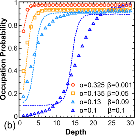
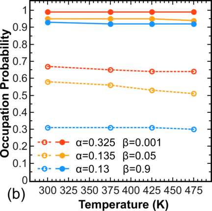
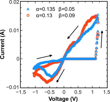
Interestingly, for parameters different from those in Figure 3.10 (α = 0.135, β = 0.05 and α = 0.13, β = 0.09) still sees a
hysteresis cycle (Figure 3.11), although the region of low occupation which, according to [72], is responsible for the rupture
of the conductive filament is almost absent. This result supports the observation that the ion dynamics is critical in
describing the RRAM switching mechanism.
3.4.3 Hysteresis cycle modeling
Time dependence
Modeling of the resistive switching in this subsection and all calculations of RRAM I - V characteristics are now
performed on a 10 × 30 two-dimensional lattice. The modeling procedure is the same as described in the
previous subsection 3.4.2. The coefficients of the boundary conditions are constant and taken to be equal to
0.1.
In order to investigate the dependence of the RESET process on time the same voltage amplitude V is applied but
different time intervals are employed. A schematic illustration of the voltages V applied is shown in the inset in Figure 3.12.
Results displayed in Figure 3.12 clearly indicate that the proper conductive filament rapture during the RESET process is
achieved, when the product “voltage-time” is maximal.
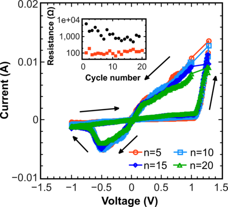
Reproducible hysteresis in RRAM
For modeling multicycle I -V characteristics a saw-tooth like voltage V has been used, where the product “voltage-time” is
maximal from the previous subsection 3.4.3. Figure 3.13 shows the hysteresis cycle obtained from the generalized stochastic
model after 5, 10, 15, and 20 cycles.
The generalized stochastic model allows enhancing RRAM endurance by properly tailoring the parameters of the cell.
The mean attenuation of the hysteresis with the number of cycles indicates that the parameters used are close to
optimal.