According to [59] the estimation for the maximum radiated electric far field
density from rectangular power planes on a PCB as depicted in
Figure 3.2 is
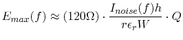 with with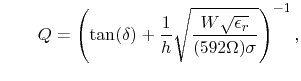 |
(3.2) |
where s is the conductivity of the planes, r is the distance of the field
observation point from the PCB,
Inoise(f) is the magnitude of the harmonic at
frequency f of the noise current Inoise,
er is the relative
permittivity, and
tan(d) is the loss tangent of the PCB substrate. Maximum
radiation occurs at the parallel plane resonances
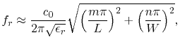 |
(3.3) |
where m and n are positive integer values and c0 denotes the speed of light in
vacuum. Note that this is a good first order estimation, intended to classify the direct
radiation of PCB planes regarding their ability to exceed an emission limit. This
estimation considers neither the influence of shields on the PCB, nor the influence of an
enclosure or the influence of the position of the noise current on the planes. The power
plane noise current Inoise has to be obtained from a network simulation which
considers the integrated circuits with ICEM models [60],
[61] and the power plane impedance. The power plane impedance for
rectangular planes is obtained from (4.18) [59]. A
powerful finite element method for the impedance simulation of fairly arbitrary shaped
planes is described in Section 4.4.
Figure 3.2:
Radiating current loop on a PCB.
|
![\includegraphics[height=6 cm,viewport=90 590 540
750,clip]{pics/Open_Edges_Estimate.eps}](img222.png) |
C. Poschalko: The Simulation of Emission from Printed Circuit Boards under a Metallic Cover