


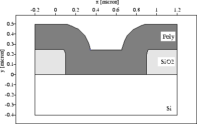
Figure 5.1-1: Initial simulation structures for a bipolar transistor with a
![]() wide single poly emitter.
wide single poly emitter.
We started up with a n-type wafer, where the collector was already
fabricated with a constant doping level of ![]() . The intrinsic
base is then implanted with boron at 35keV energy with a dose of
. The intrinsic
base is then implanted with boron at 35keV energy with a dose of
![]() into the silicon substrate. After fabrication of the
oxide isolation and a 1nm thick interfacial oxide, a
into the silicon substrate. After fabrication of the
oxide isolation and a 1nm thick interfacial oxide, a ![]() polysilicon layer was deposited at
polysilicon layer was deposited at ![]() and doped with
and doped with
![]() arsenic. The orientation of the polysilicon main
grain axis obtained from the previous deposition simulation as well as the
stress distribution in the polysilicon layer are given in
Figure 5.1-2 and Figure 5.1-3, respectively.
arsenic. The orientation of the polysilicon main
grain axis obtained from the previous deposition simulation as well as the
stress distribution in the polysilicon layer are given in
Figure 5.1-2 and Figure 5.1-3, respectively.
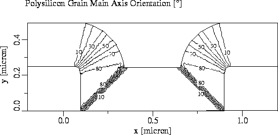
Figure 5.1-2: Orientation of the
grain main axis obtained from the deposition simulation.
The initial dopant concentration is shown in Figure 5.1-4.
During 15s RTA annealing at ![]() , outdiffusion of the arsenic dopants
from the polysilicon layer into the underlying substrate took place. The
final total arsenic distribution in the polysilicon layer as well as in the
substrate is depicted in Figure 5.1-5. The total
concentration suggests that the polysilicon grain boundaries are filled up
with dopants to their areal limit
, outdiffusion of the arsenic dopants
from the polysilicon layer into the underlying substrate took place. The
final total arsenic distribution in the polysilicon layer as well as in the
substrate is depicted in Figure 5.1-5. The total
concentration suggests that the polysilicon grain boundaries are filled up
with dopants to their areal limit ![]() . Investigating the arsenic
grain boundary concentration (see Fig. 5.1-6), we
find lower grain boundary concentrations in regions where dopant dependent
grain growth took place. The grain size determines the maximum grain
boundary concentration during annealing.
. Investigating the arsenic
grain boundary concentration (see Fig. 5.1-6), we
find lower grain boundary concentrations in regions where dopant dependent
grain growth took place. The grain size determines the maximum grain
boundary concentration during annealing.
The dopants in the grain bulk regions are totally activated, which leads to a flat profile for the arsenic grain interior concentration (see Fig. 5.1-7). Additionally, we give the lateral size of the polysilicon grains in Figure 5.1-8. Due to the high interface doping concentration a significantly increased growth rate is observed. In regions with high stress levels the growth rate is retarded.
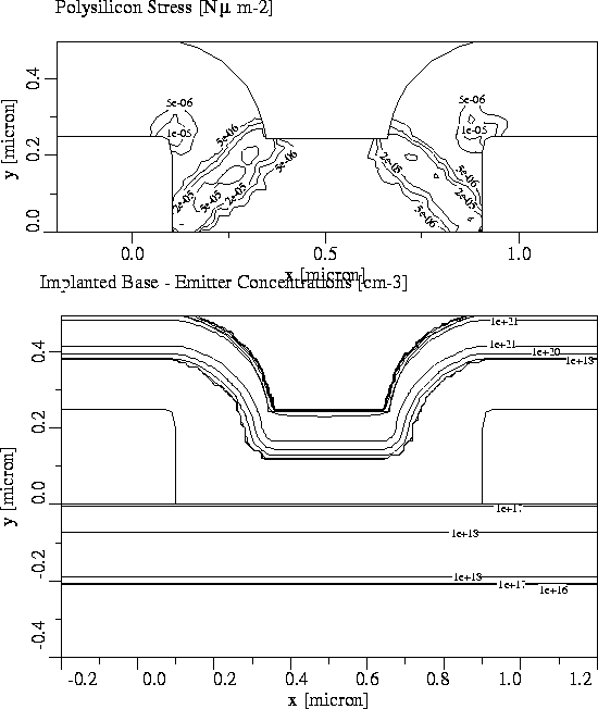
Figure 5.1-3: Stress
distribution within the polysilicon layer according to simulation geometry.
Figure 5.1-4: Initial dopant profiles after the polysilicon layer deposition
and implantation. Arsenic is shown in the polysilicon layer, where the boron
base doping is given in substrate.
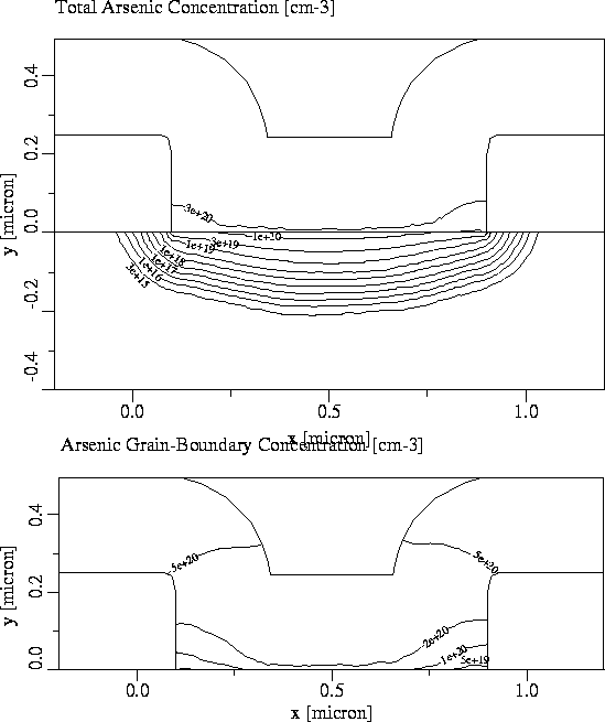
Figure 5.1-5: Resulting total arsenic distribution
after 15s RTA annealing at ![]() . In the polysilicon layer the grain
boundary and grain interior concentration was added.
. In the polysilicon layer the grain
boundary and grain interior concentration was added.
Figure 5.1-6: Arsenic
concentration in the polysilicon grain boundaries. At regions with high
grain growth rates the arsenic grain boundary concentration is lowered.
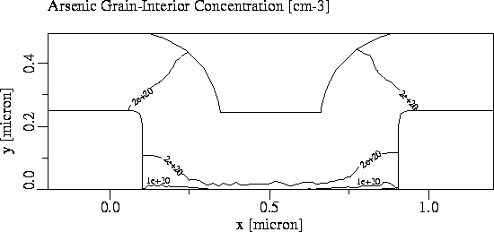
Figure 5.1-7: Arsenic
concentration in the polysilicon grains. As all dopants are activated
the distribution is nearly flat in the whole polysilicon layer.
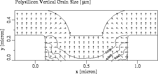
Figure 5.1-8: Vertical
size and orientation of the polysilicon grains. Enhanced grain growth starts
from the polysilicon-monosilicon interface.
The net doping concentration in the silicon substrate is given by
Figure 5.1-9, where Figure 5.1-10 gives the one-dimensional
dopant profiles of a cross-section in the mid-emitter region. The emitter
profile is high enough to achieve sufficient current gain and to keep the
emitter resistance low. The base width is 120nm and the Gummel number is
![]() .
.
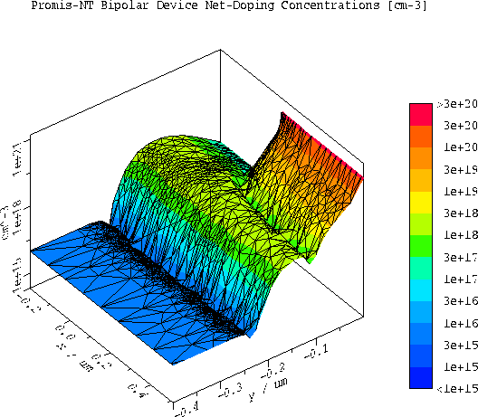
Figure 5.1-9: Net doping profile in the
active area of a NPN-transitor.
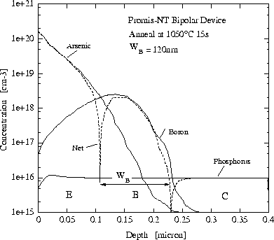
Figure 5.1-10: One-dimensional
cross-section of the dopant profiles in the mid-emitter.