


The presented ![]() BiCMOS process is performed with VISTA's
Simulation Flow Controller (SFC) [Pic93]. A tabularized process flow
including all process parameters is given in Table 5.2-2.
Each step of the flow represents a process simulation tool which reads the
last result from the previous one and performs the simulation according to
the specifications. After the tool has finished, the actual wafer state is
evaluated. This includes merging of the geometry and the doping information.
BiCMOS process is performed with VISTA's
Simulation Flow Controller (SFC) [Pic93]. A tabularized process flow
including all process parameters is given in Table 5.2-2.
Each step of the flow represents a process simulation tool which reads the
last result from the previous one and performs the simulation according to
the specifications. After the tool has finished, the actual wafer state is
evaluated. This includes merging of the geometry and the doping information.
The following simulation tools are available within the SFC:
| # | Simulator | SFC operation | Specification & Parameters |
| 1 | SKETCH | create-subdomain | create wafer: Si, p-type
|
| 2 | SKETCH | spin-on | pad oxide: |
| 3 | SKETCH | spin-on | nitride buffer: |
| 4 | SKETCH | mask | pattern buried layers: exposed, mask: 7.0, 13.5; 14.5, 22.0; |
| 5 | PROMIS | etch | open nitride |
| 6 | SKETCH | strip-material | mask |
| 7 | PROMIS | analytic-implant | N-buried layer: Sb, 200keV,
|
| 8 | TSUPREM-4 | oxidation | oxidation: SiO2, |
| 9 | SKETCH | strip-material | strip mask: resist |
| 10 | PROMIS | analytic-implant | P-buried layer: B, 75keV,
|
| 11 | SKETCH | strip-material | strip oxide: SiO2 |
| 12 | PROMIS | iso-depo | epi layer: Si |
| 13 | PROMIS | iso-depo | pad oxide: |
| 14 | PROMIS | iso-depo | nitride buffer: |
| 15 | SKETCH | mask | pattern N-well: exposed, mask: 7.0, 13.5; 14.5, 22.0; |
| 16 | PROMIS | etch | open nitride |
| 17 | SKETCH | strip-material | mask |
| 18 | PROMIS | analytic-implant | N-well: P, 150keV,
|
| 19 | TSUPREM-4 | oxidation | oxidation: SiO2, |
| 20 | SKETCH | strip-material | strip resist |
| 21 | PROMIS | analytic-implant | P-well: B, 55keV,
|
| 22 | PROMIS-NT | diffusion | well drive-in: |
| 23 | PROMIS | iso-etch | planarize |
| 24 | SKETCH | spin-on | pad oxide: |
| 25 | SKETCH | spin-on | poly buffer: poly |
| # | Simulator | SFC operation | Specification & Parameters |
| 26 | SKETCH | spin-on | nitride buffer: |
| 27 | SKETCH | mask | pattern field oxide: exposed, mask: 0.0 ,0.5; 6.5, 7.5; 13.5, 14.5; 19.5, 20.2; 21.8, 22.0; |
| 28 | PROMIS | etch | open nitride |
| 29 | SKETCH | strip-material | mask |
| 30 | PROMIS | plasma-etch | open channel stop |
| 31 | PROMIS | analytic-implant | channel stop: B, 30keV,
|
| 32 | TSUPREM-4 | oxidation | field oxide: |
| 33 | SKETCH | strip-material | strip nitride |
| 34 | SKETCH | mask | pattern subcollector: exposed, mask: 20.5,21.5; |
| 35 | PROMIS | analytic-implant | N+ subcollector: P, 180keV,
|
| 36 | SKETCH | strip-material | strip resist |
| 37 | SKETCH | mask | pattern base: exposed, mask: 14.8,19.2 |
| 38 | PROMIS | analytic-implant | intrinsic base: B, 25keV,
|
| 39 | PROMIS | iso-depo | deposit: |
| 40 | SKETCH | strip-material | strip resist |
| 41 | PROMIS | iso-etch | pregate oxide |
| 42 | PROMIS | iso-depo | gate oxide: |
| 43 | SKETCH | mask | pattern open emitter: mask: 17.6,18.4; |
| 44 | PROMIS | plasma-etch | open emitter |
| 45 | SKETCH | strip-material | strip resist |
| 46 | PROMIS | iso-depo | poly deposit: poly |
| 47 | PROMIS | analytic-implant | N+ gate/emitter implant: As, 60keV,
|
| 48 | SKETCH | mask | pattern emitter/gate: mask: 0.0, 3.1; 3.9, 10.1; 10.9, 17.1; 18.9, 22.0; |
| 49 | PROMIS | etch | form gates and emitter |
| 50 | SKETCH | mask | pattern S/D + deep collector: mask: 0.0,5.5; 7.5, 8.5;20.5,21.5; |
| # | Simulator | SFC operation | Specification & Parameters |
| 51 | PROMIS | analytic-implant | NMOS LDD S/D implant: P, 40keV,
|
| 52 | SKETCH | strip-material | strip resist |
| 53 | PROMIS | iso-depo | deposit sidewall spacer oxide
|
| 54 | PROMIS | iso-etch | sidewall etch |
| 55 | SKETCH | mask | pattern S/D + deep collector: mask: 0.0,5.5; 7.5, 8.5;20.5,21.5; |
| 56 | PROMIS | analytic-implant | NMOS S/D implant: P, 60keV,
|
| 57 | SKETCH | strip-material | strip resist |
| 58 | SKETCH | mask | pattern PMOS S/D + extr. base: mask: 5.5, 7.0; 8.5, 17.0 |
| 59 | PROMIS | analytic-implant | PMOS S/D + extr. base: B, 25keV,
|
| 60 | SKETCH | strip-material | strip resist |
| 61 | PROMIS-NT | diffusion | S/D - emitter: |
Figure 5.2-14 shows the doping profiles of the N-buried layers after an oxidation process (step 8). The grown oxide is used for the self-aligned implant of the P-buried layer. Figures 5.2-15 depicts the buried layer profiles after step 19, where additional thermal budget due to the N-well oxidation is applied onto the buried layers.
Figure 5.2-16 gives the actual dopant concentrations after the channel-stop implant (step 27) prior to the field oxide isolation, where the n-wells and the p-well doping concentrations are also given.
The final BiCMOS structure is given in Figure 5.2-17. The complexity of the simulated structure can be figured out. For further analyses we give details of all three devices.
The final PMOS device including the N-buried layer doping and the channel stop implant directly under the field oxide is given in Figure 5.2-18. The according simulation grid is shown in Figure 5.2-19 containing 7278 nodes. The n-well contact is realized by the source/drain implantation used for the NMOS device. Details of the active area dopings including the simulation grid are given in Figure 5.2-20 and Figure 5.2-21, respectively.
The NMOS device is given in Figure 5.2-22. The corresponding NMOS device exhibits a shallower buried layer doping due to the higher mobility of boron as compared to the antimony, which is used as N-buried layer dopant. The corresponding simulation grid for the NMOS device uses 7148 nodes to resolve the dopant concentrations (see Fig 5.2-23). For the source/drain fabrication of the NMOS device the well-known LDD technique is applied [Ogu80]. The active area dopings of the PMOS device as well as the corresponding simulation grid are given in Figure 5.2-24 and Figure 5.2-25, respectively.
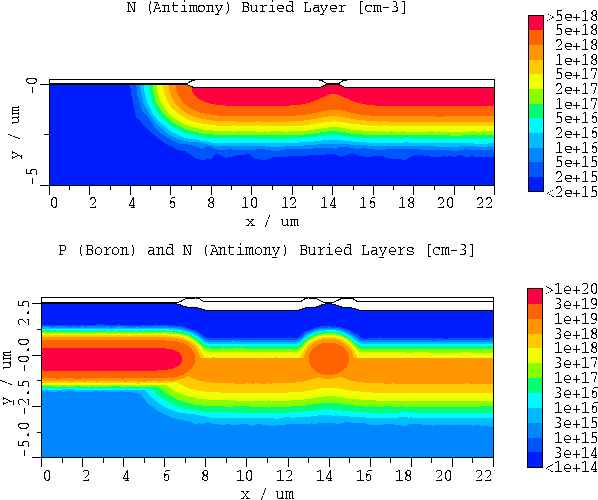
Figure 5.2-14: Simulation results
for the N-buried layers of PMOS and NPN device as result of step 8.
Figure 5.2-15: Simulation results for the P-buried
layer, the P-punchthrough and the N-buried layers obtained after step
19.
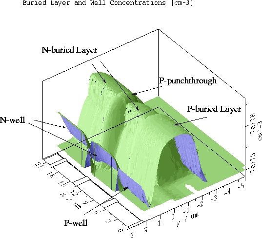
Figure 5.2-16: Simulation results for the P-buried
layer, the P-punchthrough and the N-buried layers obtained after step
19.

Figure 5.2-17: Simulation results for the final BiCMOS device
including NMOS, PMOS and NPN dopings.
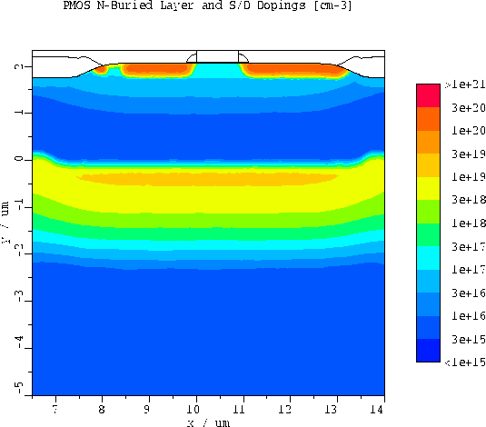
Figure 5.2-18: Simulation results for the final
structure of the PMOS device.
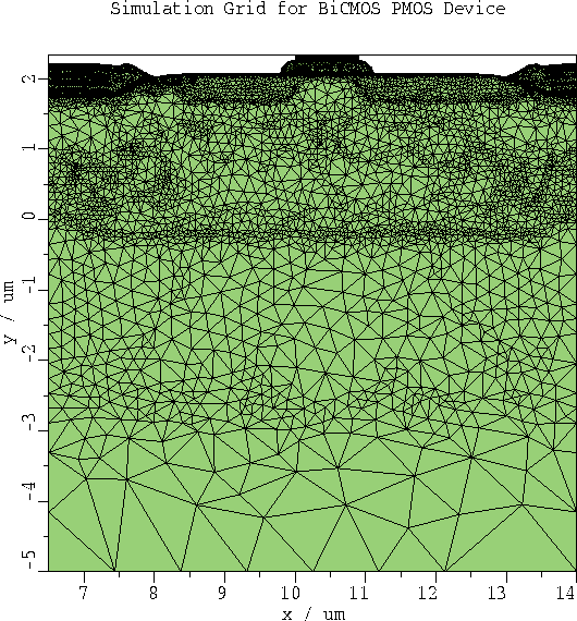
Figure 5.2-19: The simulation grid
used for the results given in 5.2-18. The grid resolves the
dopant information by using 7278 grid nodes.
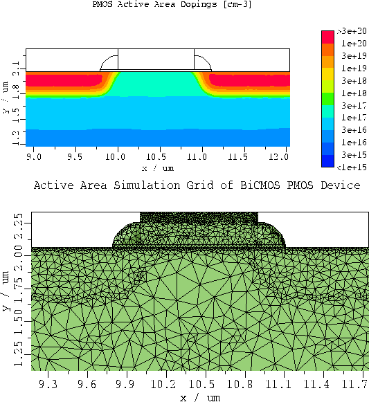
Figure 5.2-20: The active area of the PMOS
device showing source-drain dopings and N-well.
Figure 5.2-21: Details on the simulation
grid of the active area for the PMOS device.
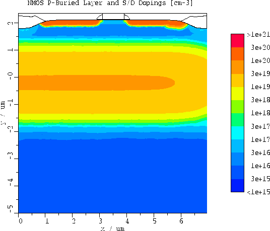
Figure 5.2-22: Simulation results for the final
structure of the NMOS device.
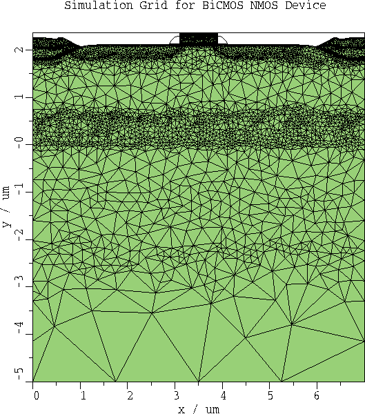
Figure 5.2-23: The simulation grid
used for the results given in 5.2-22. The grid resolves the
dopant information by using 7148 grid nodes.
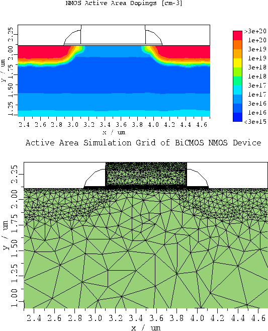
Figure 5.2-24: The active area of the NMOS
device showing LDD source-drain dopings and P-well.
Figure 5.2-25: Details on the simulation
grid of the active area for the NMOS device.
Finally, we present the bipolar NPN device structure. A lower collector contact resistance is achieved by a deep-subcollector implant. Additionally, all N-type implants during the fabrication of the active regions are applied to the subcollector. The simulation grid for the whole NPN device is given in Figure 5.2-27, where 7533 grid nodes are used to resolve the solution quantities. Due to the low diffusivity for antimony the N-buried layer changes very steep from the substrate into the epitaxial layer. The active region of the NPN device including extrinsic base, intrinsic base and emitter doping is shown in Figure 5.2-28. Details on the corresponding simulation grid are depicted in Figure 5.2-29.
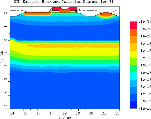
Figure 5.2-26: Simulation results for the final
structure of the bipolar NPN device.
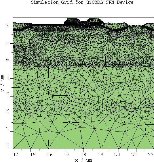
Figure 5.2-27: The simulation grid
used for the results given in 5.2-26. The grid resolves the
dopant information by using 7533 grid nodes.
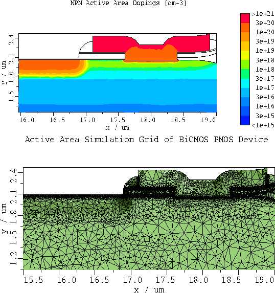
Figure 5.2-28: The active area of the NPN
device showing intrinsic and extrinsic base, emitter and collector.
Figure 5.2-29: Details on the simulation
grid of the active area for the NPN device.