


Next: 3.2.5.4 High Field Mobility
Up: 3.2.5 Carrier Mobility
Previous: 3.2.5.2 Semiconductor Alloys
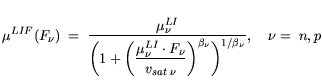
The dependence of the mobility on the driving force  is
modeled according to (3.43).
is
modeled according to (3.43).
| |
|
 |
(3.41) |
The driving force is calculated using the carrier temperature voltages  for the carrier
  .
.  is a switch
to distinguish electrons and holes which yields:
is a switch
to distinguish electrons and holes which yields:
 = -1 and
  = 1.
= 1.
The parameters for this DD high field correction are found in Table 3.16.
Table 3.16:
High-field parameters for the DD model.
| Material |
 |
 |
| III-V |
2.0 |
1.0 |
| GaN |
2.0 |
1.0 |
| Si |
2.0 |
1.0 |
|
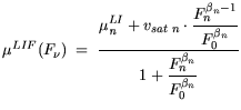
An alternative DD high field model can be applied for
electrons, which is useful for DD simulation of III-V GaAs and also AlGaN/GaN HEMTs.
In these devices negative differential mobility occurs for
fields, which is considered the extreme high field region for
GaAs or InP type semiconductors.
| |
|
 |
(3.43) |
In the model (3.45)  is considered a free
parameter contrary to (3.43), where is determined by
saturation velocity and
is considered a free
parameter contrary to (3.43), where is determined by
saturation velocity and  . For GaAs and InP,
describes the field where negative differential mobility
typically occurs. Parameter values for (3.45) are given in
Table 3.17. The comparison of shows higher values for
InP than for GaAs, while for GaN exceeds by more than an
order of magnitude. In comparison to (3.43) the determined for (3.45)
exceeds the value of
. For GaAs and InP,
describes the field where negative differential mobility
typically occurs. Parameter values for (3.45) are given in
Table 3.17. The comparison of shows higher values for
InP than for GaAs, while for GaN exceeds by more than an
order of magnitude. In comparison to (3.43) the determined for (3.45)
exceeds the value of
 / by an order of magnitude.
Table 3.17:
High-field parameters for the DD solution.
| Material |
|
|
| |
|
[V/cm] |
| GaAs |
4.0 |
4.0e3 |
| InP |
4.0 |
10e3 |
| GaN |
4.0 |
2.2e5 |
|
The model given in (3.45) is a qualitative estimate of the underlying high field physics
and is used only to match the very basic physics of GaN with the overshoot occurring at much higher fields than known from GaAs.
Next: 3.2.5.4 High Field Mobility
Up: 3.2.5 Carrier Mobility
Previous: 3.2.5.2 Semiconductor Alloys
Quay
2001-12-21