


Next: 4.2.2.2 The Parasitic Capacitances,
Up: 4.2.2 The Treatment of
Previous: 4.2.2 The Treatment of
In Fig. 4.1 a deembedding concept is indicated by the
dashed line. The line resistances
 ,
,
 , and
, and
 are
completely included in the simulation shell, since the source and
drain resistors are partly defined by the semiconductor parts of
the device, and the semiconductor-metal alloy at the ohmic
contacts. Both inductances and capacitances are considered
extrinsic. The resistances
and
are split into two
contributions which have to be evaluated for each process and
layout.
are
completely included in the simulation shell, since the source and
drain resistors are partly defined by the semiconductor parts of
the device, and the semiconductor-metal alloy at the ohmic
contacts. Both inductances and capacitances are considered
extrinsic. The resistances
and
are split into two
contributions which have to be evaluated for each process and
layout.
| |
|
 |
(4.7) |
and:
| |
|
 |
(4.8) |
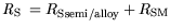
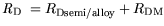
For the metal part above the semiconductor-alloy-metal transition, an additional line
resistor is added in the simulation, which is defined by the conductivity of the metal used and
the geometry of the contact to the reference plane. The metal parts of
and
,
 and
and
 , are extracted by measurements of a short structure, or alternatively by pinch-off and cold
transistor measurements [36,230,247]. DC- measurements of the ohmic resistances
were performed for reasons of control. In agreement with measurements the extracted drain resistor
can be bigger than the source resistor since at the drain side also for symmetrical devices the
electrons have to pass the heterojunction, which leads to an additional contribution. The
different ohmic contact situations were addressed in Chapter 3.
The gate resistances
have to be known very well due to their influence on noise
performance. They are dominated by the metal part of the gate, thus are determined by the width of
the single gate-finger. A line resistor
typical for the gate processing technology is
specified in the Schottky contact to obtain realistic intrinsic voltages.
is also an
important parameter for the analysis of the output conductance since for simulations including
self-heating
is a strong function of the gate temperature. The gate metal is one of the
hottest parts of the device, which leads to changes of the resistance. This is one reason for
effects such as the negative output conductance. To allow for the comparison with the resulting
bias shift on transistor performance
is modeled:
, are extracted by measurements of a short structure, or alternatively by pinch-off and cold
transistor measurements [36,230,247]. DC- measurements of the ohmic resistances
were performed for reasons of control. In agreement with measurements the extracted drain resistor
can be bigger than the source resistor since at the drain side also for symmetrical devices the
electrons have to pass the heterojunction, which leads to an additional contribution. The
different ohmic contact situations were addressed in Chapter 3.
The gate resistances
have to be known very well due to their influence on noise
performance. They are dominated by the metal part of the gate, thus are determined by the width of
the single gate-finger. A line resistor
typical for the gate processing technology is
specified in the Schottky contact to obtain realistic intrinsic voltages.
is also an
important parameter for the analysis of the output conductance since for simulations including
self-heating
is a strong function of the gate temperature. The gate metal is one of the
hottest parts of the device, which leads to changes of the resistance. This is one reason for
effects such as the negative output conductance. To allow for the comparison with the resulting
bias shift on transistor performance
is modeled:
| |
|
 |
(4.9) |
where  is the temperature coefficient of the
metal conductivity.
and
are modeled equivalently.
Typical values for the resistivity and are compiled in
Table 4.1.
For the gate composite metal a typical value of = 4
is the temperature coefficient of the
metal conductivity.
and
are modeled equivalently.
Typical values for the resistivity and are compiled in
Table 4.1.
For the gate composite metal a typical value of = 4
 is assumed.
Table 4.1:
Values for the different resistivities of IC metalization.
| Metal |
 |
|
References |
| |
[  cm] cm] |
[1/K] |
|
| Copper |
1.71e-6 |
3.9e-3 |
[82,310] |
| Au |
2.2e-6 |
3.4e-3 |
[82,173] |
| Silver |
1.55e-6 |
3.8e-3 |
[173,310] |
| Aluminum |
2.81e-6 |
3.9e-3 |
[173,310] |
| Ti |
5.54e-6 |
4e-3 |
[173] |
| W |
5.6e-6 |
4.5e-3 |
[310] |
|
Next: 4.2.2.2 The Parasitic Capacitances,
Up: 4.2.2 The Treatment of
Previous: 4.2.2 The Treatment of
Quay
2001-12-21