A 3D electrical integration system represents the entire chip divided into different blocks, which are the device layers of the chip with different functionalities.
Each block is placed on an independent silicon layer and is stacked on the top of each other by making use of the vertical dimension [131].
There are a number of approaches to arrange circuit blocks in a vertical stack to obtain 3D integration.
Based on the diverse functional requirements of each block and the processing stage during stacking, the International Technology Roadmap for Semiconductor (ITRS) proposed a classification of the wide spectrum of technologies in 3D integration [84].
There are different ways to realize 3D technologies based on their level of interconnect hierarchy and various stages of processing [150]:
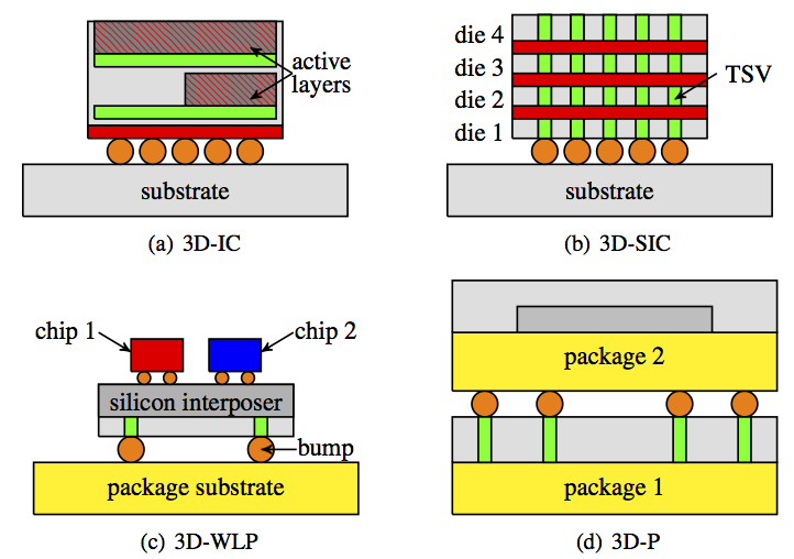
- 3D-integrated-circuit (3D-IC): integration approach which uses direct stacking of device layers using connections at the density level of local interconnects. It is generally described as the BEOL interconnect stack on multiple layers of FEOL devices during the wafer fabrication process. Since it is a process where stacked 2D device layers are connected together in the third dimension on a single semiconductor wafer, the 3D system obtained is treated as a monolithic structure, as depicted in 1.6a [122].
- 3D-stacked-integrated-circuit (3D-SIC): 3D stack which is characterized by the sequential piling-up of multiple dies or wafers using vertical interconnects at the global and intermediate levels in order to achieve communication between different stacked layers (1.6b).
These interconnects are typically TSVs with various diameters.
Usually, high-density short and thin TSVs are required at the intermediate level, while long and wide, low-density TSV structures are needed at the higher hierarchical level [122].
The integration scheme is therefore a sequence of alternating FEOL devices and BEOL layers during wafer fabrication.
Stacking approaches of ICs are die-to-die, die-to-wafer, and wafer-to-wafer [150].
- 3D-wafer-level-packaging (3D-WLP): it extends the wafer fabrication process using RDLs and bumping processes to form interconnects at the bond-pad level.
An interesting example of this strategy is the 2.5D interposer, where dies are mounted side by side on a silicon interface using TSVs through the interposer, as illustrated in 1.6c.
The TSV density requirement is typically lower than that of the 3D-SIC system.
- 3D-packaging (3D-P): integration scheme which achieves vertical stacking by relying on the traditional interconnect technologies at the package level, such as wire bonding, metal pillars, and solder bumps [106].
This includes 3D-system-in-package (3D-SiP), which is formed by stacking dies containing ICs with metal wires which are bonded to the package, and package-on-package (PoP), where the packages (SiPs) are stacked and interconnected using wire bond or flip-chip processes (1.6d).
Figure 1.6:
Schematic representations of the main 3D integration approaches: (a) 3D-IC, (b) 3D-SIC, (c) 3D-WLP, and (d) 3D-P.
|
 |
M. Rovitto: Electromigration Reliability Issue in Interconnects for Three-Dimensional Integration Technologies