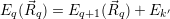
| Figure 4.2: | The |
The defect in the multi-state multi-phonon model for BTI has (at least) two structural and (at least)
two electronic configurations, as explained in Sec. 1.5. The structural reorganization of the
defect goes largely unnoticed by the rest of the system and it is only the charge state of the
defect that acts on the rest of the device via coulombic interaction. The barrier hopping
transitions 1
An overview of atomistic defect models employed for the calculation of
All three approaches have their own benefits and drawbacks. Isolated cluster models are relatively easy to set up and one can choose from the rich pool of quantum chemistry programs for the electronic structure calculation. Isolated clusters offer a simple way to treat defects that are hard to integrate into a full atomic host structure. However, they suffer from the inherent neglect of electrostatic and mechanical long range interactions.
Embedded cluster methods are an approach to improve on these drawbacks. In an embedded cluster calculation the atomistic defect model is split into three nested regions. The inner region surrounds the defect and is treated using a quantum-chemistry method. This quantum region is surrounded by the so-called classical region, which contains a large number of atoms whose interactions are described using empirical potentials [66]. Finally, the quantum-mechanical and classical regions are embedded in an infinite continuum model of the host material. Electrostatic interactions between the quantum region and the classical region are considered using the shell model for polarization on the classical atoms. In structural optimizations an inner sphere of atoms, containing the quantum region and a fraction of the classical region, is moved while the outer shell is held fixed. The atoms at the interface between the quantum region and the classical region need to be included both in the electronic structure part and in the empirical potential part of the calculation. The representation of the interface atoms in the electronic structure method is especially problematic as at least one valence electron of these atoms needs to be replaced by an interaction with the empirical potential. To account for the missing valence electron, the interface atoms are equipped with a parametrizable pseudo-potential that acts on the electrons of the quantum region. Embedded cluster methods improve upon the shortcomings of the isolated cluster calculations at the expense of a dramatically increased complexity. The set-up of an atomistic defect model using the embedded cluster approach requires a lot of fine-tuning of both the empirical potential and the pseudo-potential for the interface atom. For this reason, the embedded cluster approach is not suitable for the original study of defect parameters, but is more appropriate for refining investigations on defects for which reference calculations exist.
Supercell defect calculations have become quite popular in the solid state community. This popularity comes in part from the existence of conduction and valence levels in the calculation, and the increasing availability of plane wave based general purpose codes [102]. In the present work, we employ a supercell approach for exactly these reasons. Issues of the supercell approach include the treatment of charged cells, which will be discussed later, and interactions between the periodic images.
| | | | |
| [54] | LCLO-MO | isolated cluster | |
| [55] | Tight-Binding | isolated cluster | |
| [56, 57] | MINDO/3, MOPN | isolated cluster | |
| [58] | LSDA | supercell | |
| [159] | HF, MP2 | isolated cluster | |
| [59] | PBE | supercell | |
| [160, 161] | B3LYP | isolated cluster | |
| [162] | HF, MP2 | isolated cluster | Free relaxation |
| [77] | HF | embedded cluster | |
| [60] | B3LYP | isolated cluster | amorphous |
| [63, 163] | HF | embedded cluster | |
| [61] | PBE | supercell | amorphous |
| [64] | LSDA | supercell | |
| [65] | PBE | supercell | amorphous |
| [62] | DFT | supercell | |
| [78, 68] | HF | embedded cluster | amorphous |
| [164, 69] | B3LYP | embedded cluster | amorphous |
| [165] | PBE+HF | supercell | |
| Table 4.1: | An overview of electronic structure methods and atomistic representations employed in published defect studies. The electronic structure methods are MINDO (modified intermediate neglect of differential overlap), HF (Hartree-Fock), MP2 (second order Møller-Plesset perturbation theory), PBE (DFT with gradient-corrected functional due to Perdew and coworkers), B3LYP (hybrid DFT with gradient-corrected functional due to Becke and coworkers with HF exchange), and PBE+HF (hybrid DFT with PBE functional and HF exchange). |
| | |
| |
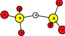
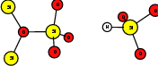
| Figure 4.1: | Atomistic defect models usually employed in calculations of point defects. All these
models attempt to describe a point defect in an otherwise ideal, infinite host structure |
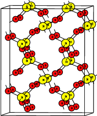
The host materials used in the studies of
To be compatible with the work of Blöchl [59], we have constructed an orthogonalized
| Figure 4.2: | The |
As two angles of the cell are already 90
| Figure 4.3: | Construction of an orthogonalized  and and  to give a 2 to give a 2 |
After the construction the atoms in the cell were relaxed keeping the cell shape and volume constant. The resulting structure is the basis for all following defect calculations and is shown in Fig. 4.4.
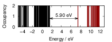
The energy cut-off for the plane wave expansion is 800eV for all calculations in this work. VASP’s
real space projection is disabled to improve the accuracy. The
| Figure 4.5: | The Kohn-Sham eigenvalue spectrum
of the |
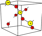
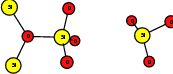
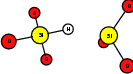
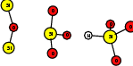
As explained in Sec. 1.6, the defect structures investigated in this work are the oxygen vacancy and the hydrogen bridge. The oxygen vacancy defect was created by removing one oxygen atom from the cell, the hydrogen bridge by replacing an oxygen atom with a hydrogen atom. Subsequent optimizations led to the dimer configuration for the oxygen vacancy and the closed configuration for the hydrogen bridge, see Fig. 4.6 and Fig. 4.7. The puckered oxygen vacancy and the broken hydrogen bridge were constructed by manual rearrangement of the defects.
Both defects give rise to one occupied state in the SiO
In the neutral state, the dimer configuration of the oxygen vacancy is more stable than the
puckered configuration by 2
The optimized structures for the oxygen vacancy and the hydrogen bridge are shown in Fig. 4.6 and Fig. 4.7, respectively. The geometries obtained from our calculations are in excellent agreement with the literature as shown in Tab. 4.2 and Tab. 4.3.
 |  |
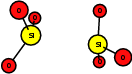 |  |
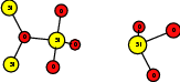
| Figure 4.6: | Structures of the dimer |
 |  |
 |  |
| Figure 4.7: | Structures of the closed |
| dimer | puckered
| |||||
| Si-Si distance | Si-Si distance | Si-O(3) distance
| ||||
| neutral | positive | neutral | positive | neutral | positive | |
| present work | 2 | 2 | 4 | 4 | 1 | 1 |
| Blöchl [59] | 2 | 3 | 4 | 4 | 1 | 1 |
| Boero [58] | 2 | 3 | | 4 | 1 |
|
| Pacchioni [159] | 2 | 3 | ||||
| Table 4.2: | Comparison of selected structural parameters of the oxygen vacancy defect in our calculations with values from the literature. |
| neutral | positive
| ||||
| present work | Blöchl [59] | present work | Blöchl [59] | ||
|
closed | Si-Si distance | 3 | 3 | 3 | 3 |
| Si
| 1 | 1 | 1 | 1 |
|
| Si | 1 | 1 | 1 | 1 |
|
|
broken | Si-Si distance | 3 | 4 | 4 | 4 |
| Si | 1 | 1 | 1 | 1 |
|
| Si | 2 | 2 | 3 | 3 | |
| Table 4.3: | Comparison of selected structural parameters of the hydrogen bridge defect in our calculations with values from the literature. |
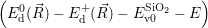
It is common in defect studies to calculate the “formation energy” of a defect. This energy is an
indicator for the abundance of the defect in thermal equilibrium. The structure of the oxide of an
MOS transistor arises from the growth kinetics of the oxidation process. Although the vibrational
state of the atoms is in thermal equilibrium with the environment, the bonding structure is not a
thermal equilibrium arrangement. Thus, the significance of the formation energies calculated here
for the abundance of oxygen vacancies and hydrogen bridges in MOS oxides is limited.
We calculate the formation energies here for the purpose of comparison with published
work. For the calculation of the formation energies it is necessary to define a “reservoir
energy” for each atomic species. The reservoir energy of the atoms is usually defined as
the gas phase energy, i.e. an isolated atom calculation [159, 66]. The formation energy
of the oxygen vacancy
| = | (4.1) | |
| = | (4.2) |
In terms of Chap. 2, the structural reorganization of the defects, i.e. the transitions 1
Our NEB calculations use ten points to sample the reaction path. The path is pre-optimized using
the conjugate gradient algorithm until forces are below 1eV
| Figure 4.8: | Reaction paths calculated using the nudged elastic band method for the
oxygen vacancy |
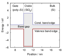
| Figure 4.9: | In a band diagram, the local values of the conduction and valence band edges are drawn as a function of position. At a material boundary, the band edges abruptly change giving rise to energetic barriers or wells. The shown band diagram corresponds to the situation in an MOS structure. |
The charge state transitions 1
The methods of semiconductor device simulation are used to model the occupation dynamics of the
extended electronic states 
 inside a semiconductor [173]. In the ground state some of these states
are occupied, and some are unoccupied. The occupied extended states
inside a semiconductor [173]. In the ground state some of these states
are occupied, and some are unoccupied. The occupied extended states 
 form the valence band of
the semiconductor, the unoccupied states
form the valence band of
the semiconductor, the unoccupied states 
 form the conduction band. Their occupation is
described by the occupation probability
form the conduction band. Their occupation is
described by the occupation probability
 | (4.3) |
The time evolution of the electronic system of the semiconductor is described by the time evolution of
the occupancy function 


 . For the holes, the quasi particle states


 . The occupancies for the excess electron and hole states are then


 . At material interfaces such as the semiconductor-oxide
interface in MOS devices, the band structure abruptly changes, leading to energetic barriers
for the carrier gas. It is common to draw the local band edges
. At material interfaces such as the semiconductor-oxide
interface in MOS devices, the band structure abruptly changes, leading to energetic barriers
for the carrier gas. It is common to draw the local band edges  ) (conduction band
edge) and
) (conduction band
edge) and  ) (valence band edge) as a function of position. These graphs are called
band diagrams and are a popular tool to illustrate processes in semiconductor devices, see
Fig. 4.9.
) (valence band edge) as a function of position. These graphs are called
band diagrams and are a popular tool to illustrate processes in semiconductor devices, see
Fig. 4.9.
In semiconductor device modeling, the materials that constitute the semiconductor device are
described using their macroscopic properties, e.g. the permittivity [175]. The coulombic interactions
in the device are accounted for in a mean field fashion by the potential Φ( ), which is obtained from
the Poisson equation
), which is obtained from
the Poisson equation
 | (4.4) |
that accounts for the charge arising from the mean density of holes
 | (4.5) |
the mean density of electrons
 | (4.6) |
and the ionized dopants  ) and
) and  ) [175]. This potential contributes to the energy of the
particles, which can be accounted for in the band diagram by replacing the band energies
by
) [175]. This potential contributes to the energy of the
particles, which can be accounted for in the band diagram by replacing the band energies
by
 | (4.7) |
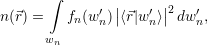
The dependence of the local band structure on the electric potential is usually termed “band bending”. The band bending as obtained from a device simulation is shown in Fig. 4.10
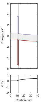 | 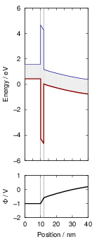 |  |
| Figure 4.10: | The mean potential Φ( ), which models the coulomb interactions within the
semiconductor device, can be described as a bending of the band structure. The band bending
as obtained from device simulation is shown for three different gate voltages (from left to right
0V, ), which models the coulomb interactions within the
semiconductor device, can be described as a bending of the band structure. The band bending
as obtained from device simulation is shown for three different gate voltages (from left to right
0V, |
The quasi particle states 
 and
and 
 as well as their occupancies are determined by the carrier
model. Depending on the complexity of the device structure, the dynamics of the excess
electrons and holes can be described at different levels of physical accuracy. The most
common carrier models, which are also employed in state-of-the-art TCAD simulators, are
based on semi-classical electrons and holes. These semi-classical particles are pictured as
wave packets of Bloch wave functions moving on classical trajectories determined by the
local band structure. The time evolution of the carriers is described using the Boltzmann
transport equation [176] in various approximations [177, 178]. The state of the carrier gas in
this description is fully characterized by the distribution
as well as their occupancies are determined by the carrier
model. Depending on the complexity of the device structure, the dynamics of the excess
electrons and holes can be described at different levels of physical accuracy. The most
common carrier models, which are also employed in state-of-the-art TCAD simulators, are
based on semi-classical electrons and holes. These semi-classical particles are pictured as
wave packets of Bloch wave functions moving on classical trajectories determined by the
local band structure. The time evolution of the carriers is described using the Boltzmann
transport equation [176] in various approximations [177, 178]. The state of the carrier gas in
this description is fully characterized by the distribution 
 ) of the electrons and the
distribution
) of the electrons and the
distribution 
 ) of the holes in the phase space (
 ). The current transport in most
semiconductor devices can be described very accurately using classical carrier models. For our
purposes, however, their applicability is somewhat limited by the inherent neglect of quantum
mechanical effects such as the quantization in the inversion channel and the penetration of
carriers into the oxide through tunneling. While this quantization has only little effect on the
prediction of transport properties, it has a profound effect on the energetics of the carrier
system, which strongly influences the carrier trapping, as will be discussed in the next
section.
). The current transport in most
semiconductor devices can be described very accurately using classical carrier models. For our
purposes, however, their applicability is somewhat limited by the inherent neglect of quantum
mechanical effects such as the quantization in the inversion channel and the penetration of
carriers into the oxide through tunneling. While this quantization has only little effect on the
prediction of transport properties, it has a profound effect on the energetics of the carrier
system, which strongly influences the carrier trapping, as will be discussed in the next
section.
Quantum mechanical carrier models can be loosely categorized into closed and open
boundary models. In the former, the Schrödinger equation for the 


Open boundary quantum mechanical carrier models are the most accurate description of the carriers in the device. These models treat the device essentially as a scattering problem. The most popular open boundary transport models are based on the framework of non-equilibrium Green’s functions (NEGF) [176]. The biggest advantage of open boundary over closed boundary models is the absence of artificial boundaries inside the device.
Independent of the physical details of the carrier model, the quantities in a semiconductor device
simulation are the average potential Φ( ), the excess electron and hole states


=  | (4.8) | |
=  | (4.9) |


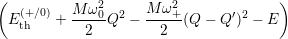
For the calculation of non-radiative transitions between the defect and the device we start from the
considerations in Sec. 2.9.2, where the general theory of NMP transitions has been laid out. The
transition rates are calculated using (2.102), which requires the determination of the electronic matrix
element and the line shape function, where the latter can either be described in the quantum
mechanical (2.94) or the classical form (2.109). To describe the phonon mediated capture and emission
of electrons and holes, it is necessary to specify the initial electronic state  i
i and the final electronic
state
and the final electronic
state  f
f for the device-defect system. The electronic structure of this system is essentially a
quantum mechanical many body problem, which we will formulate upon a basis of single
particle states. In the following,
for the device-defect system. The electronic structure of this system is essentially a
quantum mechanical many body problem, which we will formulate upon a basis of single
particle states. In the following,  d
d is the localized orbit at the defect site, and
 are the
electron states in the semiconductor device, which act as a reservoir for the transition. The
defect state as well as the reservoir states can be either unoccupied or occupied by an
electron.
are the
electron states in the semiconductor device, which act as a reservoir for the transition. The
defect state as well as the reservoir states can be either unoccupied or occupied by an
electron.
The mathematical framework for this is the second quantization formalism [183]. In the following,
the creation operators  =
=
In accord with the derivations in Sec. 2.9.2, the electronic basis states for the vibronic transition are
Born-Oppenheimer states, which are mixed by the effective non-adiabacity operator 
 | (4.10) |
The energy of the device is determined by the occupancy of the free states 
 in the valence
band and the conduction band. The energy
in the valence
band and the conduction band. The energy
![∑
HˆD = Ek [Φ (⃗r)]ˆnk.
k](thesis717x.png) | (4.11) |
The energy contribution from the electronic structure of the defect is the potential energy surface
that we obtain from our atomistic model. In the neutral (occupied) state, the potential
energy surface of the defect is  ) and in the positive (unoccupied) state it is
  ). In
addition, we have to consider the interaction of the defect with the mean potential Φ(
). In
addition, we have to consider the interaction of the defect with the mean potential Φ( ). As
we approximate the defect as a point charge at the position
). As
we approximate the defect as a point charge at the position 

 | (4.12) |
The effective non-adiabacity operator mixes the electronic states. In the device-defect system, it
annihilates an electron in a reservoir state and creates an electron at the defect state. The
corresponding single electron operators are denoted by 
 | (4.13) |
Now that all the operators are defined, one can calculate the rates for the capture and
emission of electrons from the reservoir. At first we consider the capture transition from
a reservoir state 
 , which corresponds to the removal of an excess electron from the
conduction band or emission of a hole into the valence band of the device. Initially,
, which corresponds to the removal of an excess electron from the
conduction band or emission of a hole into the valence band of the device. Initially,  d
d is
unoccupied,
is
unoccupied, 
 is occupied, and the occupancy of the other reservoir states is given by
 . The electronic system changes from the initial
state
. The electronic system changes from the initial
state
 | (4.14) |
to a state
 | (4.15) |
The energies of the initial and final state read
![E (⃗R) = ⟨i| ˆH |i⟩ = ∑ f E [Φ]+ E+ (⃗R )+ E ′[Φ]+ q Φ (⃗r )
i ′k k d k 0 d
k⁄=k](thesis736x.png) | (4.16) |
and
![∑ 0
Ef (R⃗) = ⟨f| ˆH |f⟩ = fkEk[Φ]+ E d(⃗R),
k⁄=k′](thesis737x.png) | (4.17) |
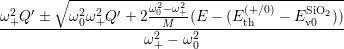
respectively. Interestingly, the energy of the captured particle as well as the mean potential at the
defect enter as an energetic shift between the potential energy surfaces before and after the capture
transition. Thus, for every reservoir state, a different configuration of the potentials is obtained leading
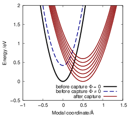
to a different NMP transition rate, see Fig. 4.11. The dependence of the energy shift on the mean
potential is responsible for the large bias dependence of the BTI defect [32, 85] as mentioned
briefly in Sec. 1.5. The dependence of the energetic shift between the potential energy
surfaces on the potential is a general feature of NMP transitions that is also present at
defects within semiconductors [144, 184]. However, for defects in the oxide this effect
dominates the field dependence of the transition as the oxide due to the large tunneling
distance between the free state and the defect. The shift induced by the oxide field in
the limit of a nearly uncharged oxide can be estimated by a simple model [185]. In this
case, the potential grows or falls linearly with the distance
| Figure 4.11: | The energy of the reservoir state from which the electron is captured as well as the mean potential in the device simulation contribute to the energetic shift between the potential energy surface of the initial and the final state. Thus, every reservoir state has a different configuration of the potential energy surfaces as indicated by the different red curves. Additionally, a change in the mean potential from the device also leads to an energetic shift, which is indicated as the blue dashed curve. |
The capture rate is now calculated from (2.102) as
 | (4.18) |
with
 | (4.19) |
As mentioned in Sec. 2.9.5, 
 | (4.20) |
where
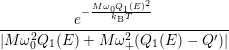
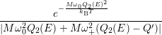
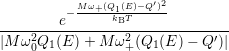
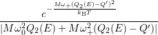
The quantum mechanical line shape is defined as (2.94)
 | (4.21) |
The energies  ) and
) and  ) as potentials,
(  ) + ) +   i i  | =  i i  | (4.22) |
(  )) )) f f  | =  f f  | (4.23) |
 i
i
 and
and  f
f
 , and trivially adds to the eigenvalues. We can
thus define the eigensystems
, and trivially adds to the eigenvalues. We can
thus define the eigensystems
 | (4.24) |
and
 | (4.25) |
which only depend on the quantities of the atomistic model. For electron capture
=  | (4.26) | |
| = | (4.27) |
 | (4.28) |
Inserting these expressions into (4.21) gives
![f = f(+ ∕0)(Ek′[Φ ]+ q0Φ(⃗rd)),](thesis773x.png) | (4.29) |
with
 | (4.30) |
The line shape as a function of energy is determined by the Frank-Condon factors 
 0
0
 as well
as
as well
as 
 | (4.31) |
In this case (4.29) becomes
![(+ ∕0) ′
f = fv (Ek′[Φ]- Ev0(⃗rd)+ q0Φ (⃗rd)) = f (Ek′[Φ ]- Ev(⃗rd)),](thesis781x.png) | (4.32) |
where 
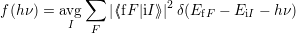
| Figure 4.12: | The line shape is referenced to the local band edges. The figure shows the position of a line shape (yellow) relative to the valence band edge (red) and the conduction band edge (blue). Different gate bias voltages lead to different band bendings and different positions of the capture line shape relative to the free quasi-particle states. In the example, the negative bias shifts the line shape maximum closer to the states near the silicon valence band edge, which is the typical NBTI situation. |
An analogous derivation can be done for the emission of an electron. In this case the electronic states are
 i i | = (  | (4.33) |
 f f | = (  | (4.34) |
| = | (4.35) | |
=  | (4.36) |
 | (4.37) |
The resulting expressions for the electron trapping and detrapping rates with respect to a state
=   | (4.38) | |
=   | (4.39) |
 | (4.40) |
The prerequisite for an electron capture from the state 
 | (4.45) |
Our approach to the calculation of NMP capture or emission rates using both a macroscopic model of the device and an atomic electronic structure model of the defect thus contains the following steps:
 ),
), 


Before we can calculate the line shapes (4.67) and (4.68), it is necessary to establish a relation between the potential energy surfaces of the atomistic model and the energy scale of the device model. This is related to the task of energy level calculation from an electronic structure method. As it turns out, there are several ways to define an energy level for a given atomistic defect model, which can be a magnificent source of confusion for the communication between theorists working on atomistic modeling and those working on device modeling. Therefore, we make an attempt here to clarify the relations of the defect levels usually given in publications to each other and to our NMP-transition based approach.
The most commonly published type of energy level calculated from atomistic defect models is the


 | (4.46) |
This formation energy accounts for the average work necessary to exchange an electron with the
reservoir. At a certain
| Figure 4.13: | Charge state formation
energies
versus electron chemical potential for a
hypothetical defect that has five charge
states ++,+,0, |
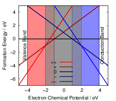
As can be seen from (4.46), the charge state formation energy depends linearly on the electronic
chemical potential and different charge states have a different slope
 | (4.47) |
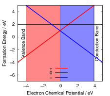
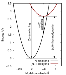
In thermal equilibrium, the thermodynamic transition level determines the dominant charge state of a defect, see Fig. 4.14.
| Figure 4.14: | The thermodynamic transition level
defines the charge state of the defect in thermal
equilibrium. If the thermodynamic transition level
of a defect is above the chemical potential the
defect is more positive, otherwise it is more negative.
Shown are different examples of possible defect states
relative to a chemical potential |
In semiconductor defect modeling, the chemical potential is commonly replaced by the electronic Fermi level. For defects with vibrational internal states, as considered in the present work, different potential energy surfaces for the various charge states lead to different vibrational spectra. In this case, a change from one charge state to another leads to a difference in the vibrational entropy of the defect [187] and thus the thermodynamic transition level of the defect becomes a Gibbs free energy [188]
 | (4.48) |
The change in the vibrational entropy of the defect thus induces a temperature dependence of the
transition level. As usually the entropy change between two charge states is small, the transition level
calculated from (4.47) is commonly considered a reasonable approximation. In the present work, we
follow the standard approach to neglect entropy for the calculation of transition levels. A special
property of the thermodynamic transition levels amongst the defect levels discussed here is that they
can describe transitions that involve the exchange of more than one electron with the reservoir. This
behavior is found in negative-U defects as illustrated in Fig. 4.15. In SiO
| Figure 4.15: | Illustration of a hypothetical
negative-U defect. The neutral state of the defect is
less stable than the charged states for all values of
the chemical potential. At |
| Figure 4.16: | The switching trap level describes the energy balance in an elastic capture process. It can be seen as a zero temperature limit of the NMP line shape. |
In addition to the thermodynamic transition level, which describes the thermal equilibrium of the
defect, a so called
 | (4.49) |
for
 | (4.50) |
for
 | (4.51) |
for
 | (4.52) |
for 
 | (4.53) |
In this case, the classical line shape function (2.109) becomes
 | (4.54) |
and via the capture and emission line shapes (4.67) and (4.68), the energy conservation expressions (4.52) and (4.51) are obtained.
The relation of the discussed transition levels to the potential energy surfaces calculated from an atomistic defect model are illustrated in Fig. 4.17.
| Figure 4.17: | The relation
of the switching and thermodynamic
defect levels to the Born-Oppenheimer
potential energy surfaces of an atomic
model of a point defect. It is assumed
that the defect structure is neutral with
|
Just as the line shapes, the thermodynamic and the switching levels require the definition of a
reference energy in order to set them into relation with the properties of the host material.
The density functional calculations in different charge states implicitly contain their own
reference level for the electrons. In the calculation of isolated molecules, the removal of
an electron from the calculation corresponds to taking the electron infinitely far away
from the molecule [99]. Thus, in isolated molecule calculations the reference level is the
vacuum level. While this referencing is reasonable for isolated molecules, in an infinite
periodic lattice the vacuum level is not a well-defined quantity and it is usually favorable to
select as reference energy one of the band edges or the midgap energy. All these energies,
however, are absent in the atomic defect models. There are different approaches to obtain
reasonable relations between the total energies of the electronic structure method and the band
edges. In principle one can use the valence or conduction level from the density functional
calculation [189, 192] as the reference. Unfortunately these levels come from the auxiliary
system and suffer from the band gap problem. A very popular method for the alignment of
the defect levels with the band edges is the so-called marker method [102, 59]. For this
approach it is necessary to have a defect with a thermodynamic transition state
 | (4.55) |
This defect is called the marker. The same thermodynamic transition level of the marker defect is calculated from the density functional calculation using (4.47). This level will be relative to the DFT zero level
 | (4.56) |
Assuming that the transition level was measured and calculated accurately, the experimental valence level in the DFT energy scale is then obtained by subtracting the two expressions as
 | (4.57) |
In our work we follow Blöchl, who uses the thermodynamic (+
| Oxygen vacancy | Hydrogen bridge
| |||
| Dimer | Puckered | Closed | Broken | |
| (+/0) thermodynamic level | 1 | 4 | 5 | 5 |
| (0/+) switching trap level | 1 | 3 | 3 | 3 |
| Table 4.4: | Thermodynamic and switching defect levels for the oxygen vacancy and the hydrogen
bridge in both structural configurations, referenced to the SiO |
Tab. 4.4 shows the thermodynamic and switching defect levels in our defect calculations using Blöchl’s energy scale alignment scheme. The calculated values are in agreement with results from the literature [59, 65, 190, 193].
As a final remark, it is worthwhile to discuss one further defect level that is sometimes given in the
literature. This defect level is the
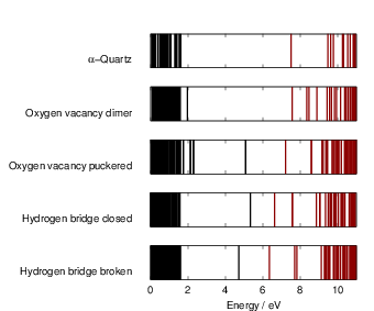
| Figure 4.18: | Kohn-Sham spectra as obtained from our defect calculations. Comparing the
spectra of the defect cells to the spectrum of the ideal |
Once an atomistic defect model and an energy alignment method is selected it is possible to calculate
line shape functions  0
0
 and
and  +
+
 and the associated energies. As
discussed in Sec. 2.9.2, for a quantum mechanical treatment of the vibronic transitions it is
necessary to approximate the potential energy surfaces of the different electronic states
as parabolas, see (2.85), which leads to a system of normal modes
and the associated energies. As
discussed in Sec. 2.9.2, for a quantum mechanical treatment of the vibronic transitions it is
necessary to approximate the potential energy surfaces of the different electronic states
as parabolas, see (2.85), which leads to a system of normal modes  ) and
) and  ) as quadratic functions.
Due to the inherent anharmonicity of these potential energy surfaces, different harmonic
parametrizations can be defined for the same defect, depending on which properties are
to be reproduced as accurately as possible [131]. In the present work, we have chosen a
parametrization that gives the same thermodynamic and switching defect levels as in the full density
functional calculation [86, 85]. Additionally, we assume here that only one mode couples to the
transition. While (2.102) is formulated upon an arbitrarily large set of coupling modes,
the exact modal spectrum obtained from the electronic structure method will generally
include some degree of mode mixing [131, 194], which requires a generalization of the
theories this work is based on. The single mode approach must be considered only a first
order approximation [144, 195]. However, the application of single effective modes is quite
common in the literature [131, 196], and it was shown quite recently that the approximation
obtained from our extraction scheme compares well to line shapes including multiple modes
[194].
) as quadratic functions.
Due to the inherent anharmonicity of these potential energy surfaces, different harmonic
parametrizations can be defined for the same defect, depending on which properties are
to be reproduced as accurately as possible [131]. In the present work, we have chosen a
parametrization that gives the same thermodynamic and switching defect levels as in the full density
functional calculation [86, 85]. Additionally, we assume here that only one mode couples to the
transition. While (2.102) is formulated upon an arbitrarily large set of coupling modes,
the exact modal spectrum obtained from the electronic structure method will generally
include some degree of mode mixing [131, 194], which requires a generalization of the
theories this work is based on. The single mode approach must be considered only a first
order approximation [144, 195]. However, the application of single effective modes is quite
common in the literature [131, 196], and it was shown quite recently that the approximation
obtained from our extraction scheme compares well to line shapes including multiple modes
[194].
In the following, we denote the nuclear optimum configuration of the neutral charge state with 


 | (4.58) |
Consequently, the mass
 | (4.59) |
The approximate potentials for the coupling mode read
=   | (4.60) | |
=   ( ( | (4.61) |
 | (4.62) |
which gives the oscillation frequencies as
=  and and | (4.63) | |
=  | (4.64) |
The resulting vibrational wave functions are harmonic oscillator wave functions (2.78)
 | (4.65) |
where 

 is the
 | (4.66) |
The line shapes of the defect are now calculated by inserting (4.65) and (4.66) into (4.31) as
= avg  | |||
  | (4.67) | ||
= avg  | |||
  | (4.68) |
 | (4.69) |
as defined in Sec. 4.5. The Franck-Condon factors 


 and
and


 are overlaps of harmonic oscillator wave functions [127]
    | = | (4.70) |
    | = | (4.71) |
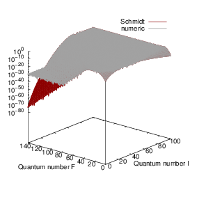
| Figure 4.19: | Comparison of the harmonic oscillator overlaps calculated by numerical integration to the recurrence relations of Schmidt [200]. For large quantum numbers the roundoff errors in the numerical integration become dominant, while the recurrence relations are numerically stable. |
| | | | |
||
| Oxygen vacancy dimer | 24 | 7 | 4 | ( | 0 |
| Oxygen vacancy puckered | 25 | 5 | 7 | (+33%) | 0 |
| Hydrogen bridge closed | 16 | 3 | 4 | (+4%) | 0 |
| Hydrogen bridge broken | 17 | 2 | 2 | (+23%) | 1 |
| Table 4.5: | Parameters of the extracted potential energy surfaces. |
Fig. 4.20 illustrates the approximate potential energy surfaces for our atomistic models of the
oxygen vacancy and the hydrogen bridge. The parameters with respect to (4.60) and (4.61) are given
in Tab. 4.5. As explained in Sec. 4.4, the relative energetic position of these potentials
depends on the reservoir state
| Figure 4.20: | Potentials for the oxygen vacancy and the hydrogen bridge (reservoir state is the silicon valence band edge). Symbols indicate the actual DFT calculations which are used to parametrize the parabolas. All defect configurations show a shift in the oscillator frequency between the two charge states, see also Tab. 4.5. |
To check the validity of our line shape calculation method, we compare our numerically calculated
line shapes to the popular formula of Huang and Rhys [127]. The Huang-Rhys line shape is derived
for linear coupling, which means that the oscillation frequency before and after the transition are the
same,
| = | (4.72) |
=   | |||
=   |
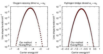
| Figure 4.21: | Comparison of our line shape calculation method that is based on harmonic
oscillator overlaps and the formula of Huang and Rhys (4.72). The energy scale is referenced
to the silicon midgap energy. The Huang-Rhys formula is limited to linear coupling, i.e. the
oscillation frequencies before and after the transition are the same. In this example we use |
For the calculation of the line shapes we have considered 200 neutral and 200 positive states.
The line shape functions as calculated by (4.67) and (4.68) are a series of weighted Dirac
impulses, see Fig. 4.22. These Dirac peaks, however, are artifacts of the time dependent
perturbation theory that is used to calculate the rates. This approach assumes that at
| Figure 4.22: | Line shapes |
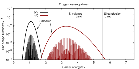
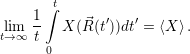
The line shape functions for all transitions are shown in Fig. 4.23, which shows that stronger
bonds in the initial state lead to sharper line shape peaks. The bond of the oxygen vacancy
dimer is weakened by hole capture, so the
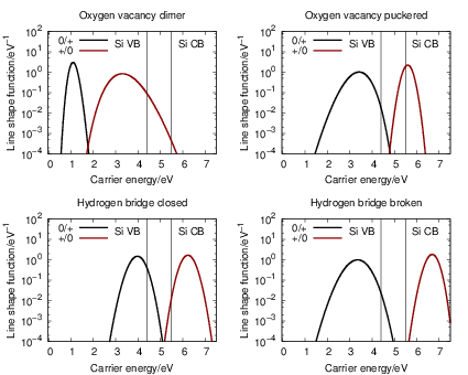
| Figure 4.23: | Emission and capture line shape functions at 300K for the oxygen vacancy and
the hydrogen bridge. Two hundred eigenstates in both the neutral and the positive defect state
have been considered for the calculation of the line shapes. The energy scale is referenced to
the SiO |
Fig. 4.24 shows the temperature behavior of the (0
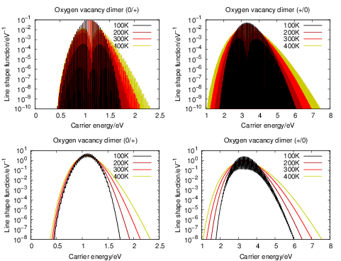
| Figure 4.24: | Quantum mechanical line shapes of the oxygen vacancy dimer both before
|
As discussed in Sec. 2.10, line shapes can also be calculated based on classical statistical physics. In the defect-device system, the shift induced by the mean field and the free state enters directly into the energy conservation expression. Again we can define the defect line shapes
= 
  | (4.73) | |
= 
  | (4.74) |
= 
 | (4.75) | |
= 
 | (4.76) |
Inserting the one dimensional potentials (4.60) and (4.61) into (4.73) and (4.74) yields
= 
 | (4.77) | |
= 
 | (4.78) |
= 
 | (4.79) | |
= 
 | (4.80) |
 | (4.81) |
where the
 | (4.82) |
=   + +   | (4.83) | |
=   + +   | (4.84) |
| Oxygen vacancy dimer |
 |
| Hydrogen bridge closed |
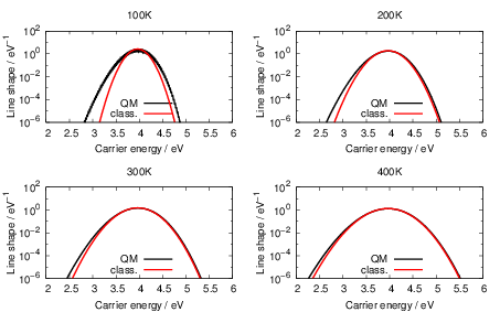 |
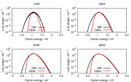
| Figure 4.25: | Comparison of the classical line shapes from (4.84) to their quantum mechanical counterparts that were calculated numerically from (4.68) at the indicated temperatures for the dimer configuration of the oxygen vacancy and the closed hydrogen bridge. Deviations between the two versions arise at low temperatures and in the weak coupling regime (energies below the peak of the line shape) due to the absence of tunneling in the classical version. |
The classical
When quantum effects are negligible, however, it is also possible to calculate line shapes with the
full potential energy surfaces from the density functional calculations. Quite generally, the integrals of
a function  ) of the form
 | (4.85) |
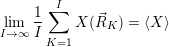
are called “thermal averages” of the canconical ( . As the
potential
. As the
potential  ) that determines the weighting factor for the averaging is usually a function of low
symmetry in
) that determines the weighting factor for the averaging is usually a function of low
symmetry in 


 ) over the set of sample points will approach the true average of the canonical
ensemble
) over the set of sample points will approach the true average of the canonical
ensemble
 | (4.86) |
The Metropolis Monte Carlo algorithm is broadly applied in atomistic modeling to calculate thermally influenced properties as bond lengths, free energies, etc. and its general formulation makes it possible to include a particle reservoir and pressure in addition to a thermal reservoir [120, 112, 203].
The molecular dynamics method on the other hand tries to describe the dynamics of the
molecular system by propagating the positions of the nuclei according to Newton’s equations of
motion [119, 120]. In its pure form, the method just generates the constant energy trajectory of an
atomic system from a given starting point in phase space [119], which corresponds to the
microcanonical (
 | (4.87) |
(
The classical line shapes can also be written as thermal averages
=   ) )  | (4.88) | |
=   ) )  | (4.89) |
 | (4.90) |
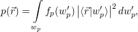
As mentioned in Sec. 2.10, these averages give the probability that for a given carrier energy  )
)  )
)
We have tested this calculation method for the closed hydrogen bridge. For the generation of the
trajectory, we use the molecular dynamics implementation of VASP, which implements a Nosé
thermostat [112]. Due to the large computational demand of the molecular dynamics calculation, the
accuracy of the density functional calculation is reduced here, using a plane wave cut-off of 500eV and
the real space projection feature of VASP. We calculate the
| Figure 4.26: | Comparison of the line shapes for the closed hydrogen bridge as calculated from the approximate harmonic potential energy surface in the classical and quantum mechanical form to the line shapes calculated from molecular dynamics. Excellent agreement between the different calculation methods is found around the maximum of the line shape. |
The result is shown in Fig. 4.26. Excellent agreement is found between the line shapes calculated
from molecular dynamics and from the approximate potentials around the maximum and above. We
take this result as an indication for the validity of the harmonic approximation. The calculation of line
shapes from molecular dynamics or Metropolis Monte Carlo is undoubtedly an appealing
approach as it includes all features of the density functional potential energy surfaces.
Its applicability to the calculation of line shapes for BTI, however, is limited by the long
trajectories that have to be calculated in order to get smooth line shapes further away
from the maximum. The line shape in Fig. 4.26 is only smooth to about 0
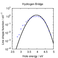
| Figure 4.27: | Comparison of the line shapes extracted from density functional theory based on
the PBE functional and the PBE0 functional. Except for the (0 |
The PBE gradient corrected functional we employ in our work is quite popular in solid state theory.
However, adding a fraction of Hartree-Fock exchange to the density functional calculation improves
the description of band gaps and other properties of many atomic systems [192, 99]. We have
checked the dependence of the calculated line shapes on the employed functional by comparing our
PBE results with calculations using the PBE0 hybrid functional. Due to the high computational effort
that is required with hybrid functionals, we only investigated the primary states of our model
defects, i.e. the oxygen vacancy in its dimer configuration and the closed hydrogen bridge. A
comparison between the PBE and PBE0 prediction of the defect levels for the model defects
considered here has been done by Alkauskas et al. [204]. This comparison found that the
defect levels were largely shifted by about 1
The biggest uncertainty in our calculations comes from the alignment of the energy scales between the
atomistic defect model and the free charge carrier states in the semiconductor device. Although the
marker method performs well for defects that are sufficiently similar to the marker defect [102], the
accuracy of the alignment depends heavily on the accuracy of the experimental reference values.
Blöchl’s placement of the (+
In the multi-state multi-phonon model for BTI, the more stable configurations in the neutral state and
the positive state are 1 and 2, the metastable configurations are 1
| 1 | 1 | 2 | 2 | |
| Oxygen vacancy | 3 | 36 | 0 | 0 |
| Hydrogen bridge | 1 | 1 | 0 | 0 |
| BTI defect [206] | | | | |
| Table 4.6: | Activation energies for the structural reconfigurations as calculated from the atomistic defect models using the nudged elastic band method. |
The reaction paths for the 1
For the discussion of the charging and discharging reactions 1
The maximum of the hole capture line shape of the closed hydrogen bridge on the other hand is too
close to the silicon valence band to show the BTI behavior. The widening due to an increase in the
temperature as well as the bias dependence are stronger for carriers further away from the line shape
maximum. In the shown configuration, both the bias and the temperature dependence are weak, which
unfortunately does not match the properties of the BTI defect. However, the calculations in [193]
showed a spread for the (0
While the line shape of a defect includes the quantum mechanical effects, and the dependence on
the reservoir state energy and the band bending, it does not give any information about
the temperature behavior. However, as mentioned in Sec. 4.7, the activation barrier for
the charge state transition can be estimated from the intersection of the potential energy
surfaces. The parabolic approximations extracted from our density functional calculations are
shown in Fig. 4.20, where the energy of the involved free state is placed at the silicon
valence level. This corresponds to the most dominant energetic configuration for hole capture
with no field in the oxide. It can be seen that in the primary (dimer) state, the oxygen
vacancy has to overcome a large thermal barrier to capture a hole from the silicon valence
band edge, which corresponds to the small value of the line shape at this energy. The
temperature activation of the 1
Only minor changes to the line shapes are observed when moving from the PBE to the PBE0
functional, except for the (0

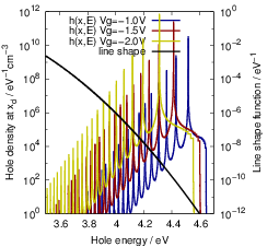
| Figure 4.28: | The spatially and energetically distributed hole density as calculated using the NEGF method. Thermal equilibrium in the gate and the silicon bulk is induced via an optical potential. The quantization of the hole states and their penetration into the oxide can be clearly seen. |
Once the line shapes are calculated and an accurate device simulation method is
selected, one can proceed to calculate capture and emission rates using (4.41)–(4.44). In
the present work, the carrier concentration of the MOS structure has been calculated
self-consistently using the non-equilibrium Green’s function method [207]. The densities 


We have implemented the rate calculation directly into the VSP2 simulator. The calculation of the NMP hole capture rates proceeds in a two step process. First, the band bending is calculated by solving the Poisson- and the NEGF equations self-consistently. Secondly, the NEGF problem is again solved non-self-consistently on a different energy grid that accounts for high energy holes as these contribute considerably to the NMP transitions. The integration is implemented as a post-processing step using the numerical NEGF and line shape data.
At the time this thesis is written, the transition rate calculations involving unoccupied states in the
device, corresponding to hole emission and excess electron emission, is still work in progress. Of the
transitions involving occupied states, corresponding to carrier capture, the hole capture transition is
most important for the present work. For this reason we concentrate on the calculation of hole capture
rates using (4.42). Due to the empirical factor
| Figure 4.29: | Illustration of the
bias induced shift of the relative
position of the line shape and
the free hole states. The   |
First, we investigate the effect of the bias induced shift of the relative positions of the line shape and the hole states. As mentioned in Sec. 4.4, this shift is especially relevant for the trapping behavior of oxide defects. Application of a gate voltage induces the largest electric field, and in consequence the largest band bending, in the oxide due to the absence of native carriers there. As illustrated in Fig. 4.29, the dependence of the line shape on the value of the reference energy at the defect site plays a crucial role for the transition kinetics, as the band bending energetically shifts the relative position of the line shape and the spectrum of the hole states, leading to large changes in the capture rate.
In semiconductor device modeling, defects are primarily considered as recombination centers and
described using the Shockley-Read-Hall (SRH) theory [209], which characterizes a defect via the
capture cross section
=  | (4.91) |
= 
| (4.92) |
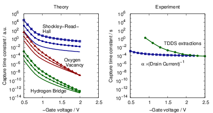
| Figure 4.30: | |
Fig. 4.30 left shows the gate voltage dependence of the NMP hole capture time constants for the two model defects. The gate voltage dependence predicted from the NMP theory is much stronger than the prediction of th SRH-like model. Further, the gate voltage dependence increases with the distance of the defect from the silicon bulk. Both of these strong dependencies are caused primarily by the energetic shift of the line shape functions relative to the holes in the inversion layer, as illustrated in Fig. 4.29. This behavior is in qualitative agreement with the capture rates observed in TDDS measurements. As explained in the previous section, the agreement would not be as good in the originally selected energy alignment scheme.
| Figure 4.31: | Arrhenius plots of the capture rates for the defect types comparing the quantum mechanical NMP capture rates (4.68) for the puckered oxygen vacancy and the closed hydrogen bridge to the capture rates calculated using classical atoms (4.84) and to a SRH like model. The indicated activation energies are obtained by fitting to an Arrhenius law. |
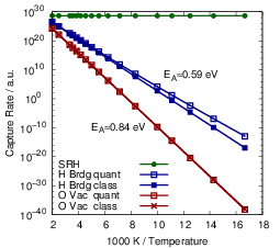
The temperature dependence of the hole capture is shown in Fig. 4.31. The calculation of NMP hole capture rates for the given defects becomes numerically challenging for low temperatures. As the temperature decreases, the line shapes become increasingly narrow, thus making high energy holes the dominantly captured particles. Accurate representation of high energy holes in the NEGF algorithm requires an improved refinement strategy for the energy grid, which is currently under development. To overcome this limitation, the hole distribution over energy was calculated from a classical density of states for the Arrhenius plot, taking only the total hole concentration at the defect site from the NEGF calculation.
NMP defects show a strong temperature activation, in contrast to capture rates whose temperature dependence comes from the total carrier density alone, as in the SRH description. The calculated activation energies for the hole capture are in excellent agreement with the activation energies obtained from TDDS experiments in [32], which is again strongly influenced by the selected alignment scheme. The difference in temperature activation between line shapes calculated using the quantum mechanical formula of (4.68) and those calculated based on classical statistical physics (4.84) are also compared in Fig. 4.31. For the closed hydrogen bridge, this difference becomes visible only below 140K. For the puckered oxygen vacancy, the classical formula reproduces the quantum mechanical behavior over the complete temperature range investigated. Again, we take this as an indication that the quantum mechanical effects of the nuclei are negligible for the calculation of rates of typical BTI experiments.
NMP theory has been used by several authors in the context of semiconductor devices [144, 180, 181, 202, 32, 182]. The transition rate formulas employed are usually based on linear electron-phonon coupling. As shown in Fig. 4.20, this assumption is not fulfilled for our density functional based defect models. Purely quadratic coupling has been investigated in the literature [128, 129], but a linear-quadratic coupling that changes both the equilibrium position and the frequency of the coupling mode has not been considered up to now.
With respect to the modal spectrum, it is either assumed that the transition couples to an infinite number of phonon modes — all having the same oscillator strength — where each can contribute only one phonon [127, 202, 181], or that the transition couples to only one effective mode which receives or emits an arbitrary number of phonons [144, 117, 131]. Interestingly, for linear coupling modes both assumptions lead to essentially the same expression for the capture rates. For the situation we find in the bias temperature instability, in our opinion it is more reasonable to assume that the NMP kinetics are determined by a small number of local modes at the defect site. A coupling to a large number of modes does not seem reasonable for the defects involved in BTI and RTN considering the large variations in transition rates between the defects that are observed in measurements. These variations can only be explained by differences in the local environment of the defect structure which can only hold a small number of vibrational modes.