 750
750 m). Hence, in addition to the TSV building, a
polishing process is needed to reduce the wafer thickness. After polishing, the wafers
(or die) are aligned and piled upon each other using a bonding process shown in
Fig. 1.6.
m). Hence, in addition to the TSV building, a
polishing process is needed to reduce the wafer thickness. After polishing, the wafers
(or die) are aligned and piled upon each other using a bonding process shown in
Fig. 1.6.
TSVs are big vertical interconnections, usually made of metal. The structure can be bulky (filled TSV) or hollow (unfilled TSV) depending on the design and process requirements. TSV fabrication can be split in 4 steps: Etching, metal deposition, wafer thinning, and bonding [30][31].
The Bosch process is usually employed to etch the planned TSVs wells, but other processes
such as Non-Bosch DRIE and Laser drilling can be used. Subsequently, a metal or poly-Si is
deposited in order to create the conduction path inside the via. However, it is very
tough to produce a TSV which is long enough to go through the entire depth of
a commercial wafer (750m). Hence, in addition to the TSV building, a
polishing process is needed to reduce the wafer thickness. After polishing, the wafers
(or die) are aligned and piled upon each other using a bonding process shown in
Fig. 1.6.
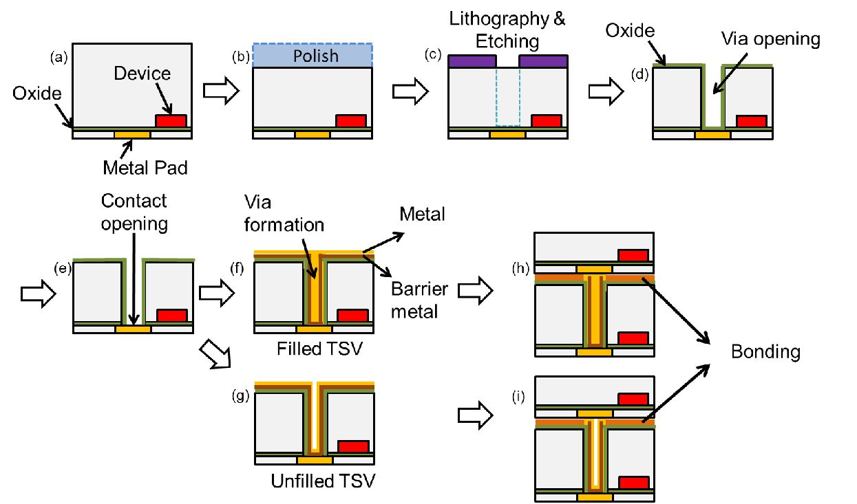
| Figure 1.6.: | Typical processing of a TSV. A Die (or wafer) ready (a) for TSV manufacturing is polished (b) on its backside to reduce the thickness. In the following, the sample is structured by photolithography (c) and the via hole is etched (d). Then, the metal pad is exposed (e) and the conduction metal is deposited (f and g), accordingly to the TSV type. Finally, the die (or wafers) are stacked and bonded. |