Next: 4.3.2 Comparison of Interface State Profiles Extracted with Different Capacitance Approaches Up: 4.3 Charge-Pumping Extraction Techniques Previous: 4.3 Charge-Pumping Extraction Techniques
All considered methods employ the oxide capacitance Cox as a key parameter of the extraction procedure. In the methods derived by Mahapatra [66] and by Li [179] Cox is treated as a constant
where tox is the oxide thickness at the device center and εox the dielectric permittivity.This approach is applicable only for transistors with a fixed oxide thickness and leads to erroneous results when tox depends on interface coordinate x. Moreover, even in the case of uniform thickness distribution, such a scheme leads to spurious results. In fact, in such an approach the capacitor is considered ideal i.e. the electric field is assumed uniform. In work of Chim et al. [177] it was possible to find an extension of (4.14) when tox depends on x (tox = tox(x)). In practice, however, a substantial distortion occurs near the source/drain ends of the gate. The aforementioned simplification does not strongly affect the transistor characteristics. However, the electric field non-uniformity is of particular importance for the extraction of the interface state density profile after HC stress because Nit(x) peaks near the drain end of the gate where the capacitor non-ideality is most pronounced [41]. Additionally, Lee et al. [178] have already demonstrated that the coordinate dependence of the capacitance Cox(x) due to the fringing effect is essential.
|
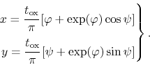
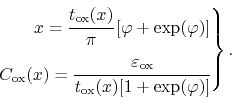
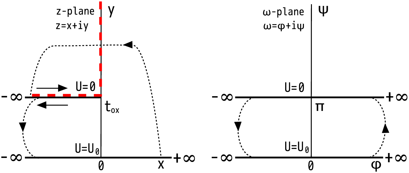
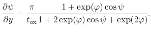
The conformal-mapping method is most helpful for the calculation of the fringing electric field in simple two-dimensional boundary problems (which is our case) by transforming the boundary to a soluble form [184]. A series of simulations based on the Lee et al. approach [178] (described below) allow us to draw the conclusion that, for a local oxide capacitance consideration, a simplified structure can be used. Namely, the gate contact can be interpreted geometrically as a ray instead of more complicated corner variants. The problem with the coordinate system is shown in Figure 4.11. Here, the origin of the considered system is placed at the drain end of the gate. The z = x+iy plane is mapped into the ω = φ+iψ plane with the functional relationship between z and ω described by
 |
(4.15) |
The suggested conformal transformation shown in Figure 4.11 reduces the pristine problem to the Laplace problem between two parallel infinitely long metallic plates at different potentials [184]. The analytical solution for the potential and the electric field distribution in the oxide near the gate end following from the conformal map and that obtained by MiniMOS-NT are presented in Figure 4.12. One can see a rather good agreement between the obtained results which means that the chosen geometrical system interpretation is correct.
 |
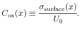
The local oxide capacitance can be defined as the ratio between the surface charge density σsurface and the interface potential U0, written as
That is, for the determination of the local oxide capacitance it is first of all necessary to find the surface charge density σsurface. According to [185]
 |
(4.18) |
 |
(4.19) |
 |
(4.20) |
 |
(4.22) |
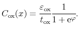
It should be mentioned that in (4.23) the parameter tox has been changed to tox(x). As reported in [185], this substitution is legitimate until dtox(x)/dx which is correct for devices with a real topology of the gate contact. The value of Cox(x) in (4.23) has a maximum with Cox(= εox/tox) in the middle of the gate and decreases gradually toward a much lower value outside the gate edge due to the fringing effect. At x→-∞ (or φ→-∞) the obtained equation (4.23) asymptotically turns into an expression for the parallel-plate capacitance (4.14).
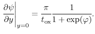
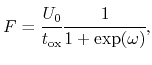
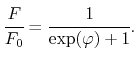
It is rather important to clarify at which distance from the drain edge of the gate contact the electric field becomes uniform. In other words, where the fringing effect is negligible and the parallel-plate capacitor approximation is applicable. For this purpose let us find a position on the x-axis where the electric field intensity differs by 1% from the uniform one, i.e F0 = U0/tox [184]. For any position of consideration in the Figure 4.11 system, the electric field intensity can be defined using the employed conformal transformation as F = |dω/dz|. Therefore, from (4.21) one may conclude
 |
(4.24) |
 |
(4.25) |
Assuming F/F0 = 0.99 we obtain exp(φ) = 0.0101 and, consequently, φ = -4.61. A substitution of the obtained values in the expression for the x coordinate in (4.16) results in
 |
(2.26) |
Here, x = Lg is the position of the drain end of the gate. Thus, one cane consider the local oxide capacitance as constant (i.e. use the parallel-plate capacitor approximation) already at a distance of 1.47 of the oxide thickness at the drain end of the gate contact. As a result, it is possible to operate with a simple expression (4.14) if the region of interest is outside of the mentioned area.
For evaluating the local oxide capacitance using device modeling we employ the method suggested by Lee et al. [178]. To determine the Cox(x) by means of simulations, a careful calculation of the local flatband Vfb(x) and threshold Vth(x) voltage distributions is performed. Due to the symmetry of the source and drain for the fresh device, one presents results only for the drain half of the device [178]. As mentioned in Section 4.1, for an unstressed transistor the Vth(x) and Vfb(x) profiles can be obtained by the device simulator MiniMOS-NT. For any point on the device interface the post-stress local threshold Vth(x) and local flatband Vfb(x) values are related to the pre-stressed ones by (4.13) which considers the change between pre- and post-stress concentrations of interface traps and bulk oxide charges. The presence of a uniform probe oxide charge Not,uniform leads to a local threshold voltage shift ΔVth,uniform(x) = Vth,s(uniform)(x) - Vth(x) [178]. Therefore, the local oxide capacitance can be found using
 |
(2.27) |
A typical example of ΔVth,uniform(x)) induced by a uniform oxide charge density of 5×1011cm-2 is shown in Figure 4.13a.
(a)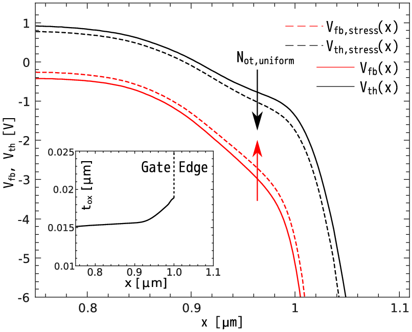 (b)
(b)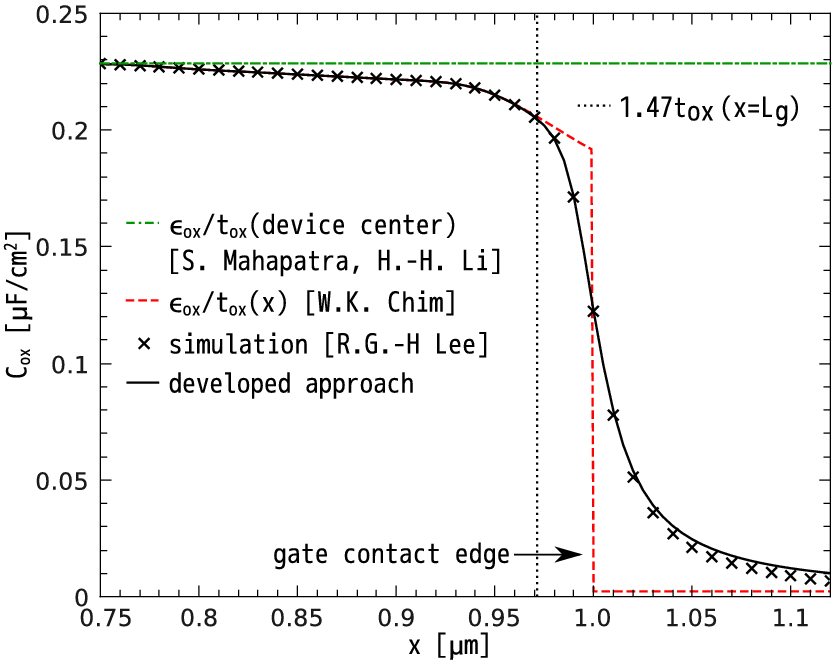
|