|
|
|
|
Previous: 3.4 Basic Properties of the Diamond Structure Up: 3.4 Basic Properties of the Diamond Structure Next: 3.5 Effect of Strain on Symmetry |
The band structure describes the variation of the energy ![]() with the
wave-vector
with the
wave-vector
![]() . The valence bands contain the last filled energy levels
at
. The valence bands contain the last filled energy levels
at ![]() K, whereas the conduction bands are empty at
K, whereas the conduction bands are empty at
![]() K. The band gap
K. The band gap
![]() separates the conduction band
from the valence band. The band structure is usually visualized by plotting
separates the conduction band
from the valence band. The band structure is usually visualized by plotting
![]() on symmetry lines, where
on symmetry lines, where ![]() denotes the band index. In
Figure 3.6 the band structure of Si is plotted on the
symmetry lines given in (3.27).
denotes the band index. In
Figure 3.6 the band structure of Si is plotted on the
symmetry lines given in (3.27).
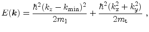
The band structure close to the conduction band edge can be approximated by
ellipsoidal energy surfaces and a parabolic energy dispersion
![]() . In Si the conduction band edge is located near the zone boundary
. In Si the conduction band edge is located near the zone boundary ![]() points along the
points along the ![]() symmetry lines. For the conduction band valley at
symmetry lines. For the conduction band valley at
![]()
![]() the energy dispersion reads
the energy dispersion reads
Due to the point symmetry of the fcc lattice the six directions ![]() ,
,
![]() ,
,![]() ,
,
![]() ,
,![]() , and
, and
![]() are
equivalent. Consequently, there are six conduction band valleys. The constant
energy surfaces of all six equivalent valleys along the principal axes
are
equivalent. Consequently, there are six conduction band valleys. The constant
energy surfaces of all six equivalent valleys along the principal axes
![]() are shown in Figure 3.7. Since electron transport in unstrained
Si involves the electrons moving in all of the six valleys, it shows little
anisotropy, even though there is strong anisotropy in each valley.
are shown in Figure 3.7. Since electron transport in unstrained
Si involves the electrons moving in all of the six valleys, it shows little
anisotropy, even though there is strong anisotropy in each valley.
[a]![\includegraphics[width=2.6in]{xmgrace-files/Si_bandstructure.eps}](img299.png) [b]
[b]![\includegraphics[width=2.6in]{xmgrace-files/Si_Vbandstructure.eps}](img300.png)
|
![\includegraphics[scale=1.0, clip]{inkscape/bzEle.eps}](img301.png)
|
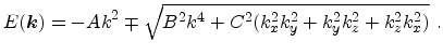
The valence band edge is located at the ![]() point, where the heavy hole
(HH) and light hole (LH) band are degenerate. The split-off band (SO) is very
close, since the split-off energy is only 44 meV in Si. For very
small energies constant energy surfaces can be approximated by
point, where the heavy hole
(HH) and light hole (LH) band are degenerate. The split-off band (SO) is very
close, since the split-off energy is only 44 meV in Si. For very
small energies constant energy surfaces can be approximated by
|
|
|
|
Previous: 3.4 Basic Properties of the Diamond Structure Up: 3.4 Basic Properties of the Diamond Structure Next: 3.5 Effect of Strain on Symmetry |