Next: 5.1.4 Optimization Techniques Up: 5.1 Depletion-Mode HEMTs Previous: 5.1.2 High Temperature Simulations Contents
One of the difficulties, which still hampers the wide use of HEMTs, is
the very strong dependence of the transconductance on the gate
voltage. As the derivatives of the transconductance with respect to the
gate voltage are detrimental to intermodulation distortion
[384,19], a profound knowledge of the causes for the
transconductance nonlinearity significantly helps the selection of a
proper load resistance. The problem has been addressed in numerous
works, e.g. [385,386]. Interface roughness and hot-phonon
scattering have been ruled out as possible reasons for the strong
dependence of the transconductance on gate voltage. While real space
transfer effects are relevant in GaAs-based pHEMTs [370], the
lack of a significant leakage current in the studied structures counts
against it. Recently, the decrease of transconductance has been
attributed to the strong nonlinearity of the source-gate
resistance. This has been shown in a couple of studies relying on
experimental measurements combined with simulations
[385,386], which employ specially tailored carrier velocity
![]() electric field characteristics. Here, a good agreement with
experimental data is achieved by using electron mobility Model B based
on Monte Carlo simulation results. The electron transport in the
source-gate and gate regions is studied in a wide range of gate-source
voltages and the impact of scaling the source-gate distance
electric field characteristics. Here, a good agreement with
experimental data is achieved by using electron mobility Model B based
on Monte Carlo simulation results. The electron transport in the
source-gate and gate regions is studied in a wide range of gate-source
voltages and the impact of scaling the source-gate distance
![]() on
transistor performance is discussed [19]. It is
shown that the transconductance decrease should not be attributed to
negative differential mobility effects, which is also reproduced by
using a velocity-field characteristics from MC simulation
results. Device C is used for the study with
on
transistor performance is discussed [19]. It is
shown that the transconductance decrease should not be attributed to
negative differential mobility effects, which is also reproduced by
using a velocity-field characteristics from MC simulation
results. Device C is used for the study with
![]() , which has been
already described in the previous sections.
, which has been
already described in the previous sections.
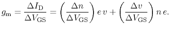
Fig. 5.25 shows the measured and simulated transfer characteristics of the device. Without any changes in the models or model parameters a very good agreement is achieved for the drain current as well as for the transconductance. The simulated transconductance exhibits roughly the same maximum value as the measurement and adequately follows the decrease at higher gate voltage. In order to gain a better understanding of the carrier transport process in the device, the transconductance can be expressed as:
The first term describes the contribution of the change in carrier
concentration ![]() . The simulations show that it is substantial
only under the gate, as in the source-gate and gate-drain areas no
variation of the carrier concentration with
. The simulations show that it is substantial
only under the gate, as in the source-gate and gate-drain areas no
variation of the carrier concentration with
![]() is
observed. The rapid increase in concentration in the bias range near
the maximum transconductance combined with a high electron velocity
(Fig. 5.26) indeed results in some contribution of this
term to the overall
is
observed. The rapid increase in concentration in the bias range near
the maximum transconductance combined with a high electron velocity
(Fig. 5.26) indeed results in some contribution of this
term to the overall
![]() . However, this contribution is limited to a
small area under the gate in a narrow voltage range, therefore for the
further studies we focus primarily on the second term (the change in
carrier velocity
. However, this contribution is limited to a
small area under the gate in a narrow voltage range, therefore for the
further studies we focus primarily on the second term (the change in
carrier velocity ![]() ).
).
Fig. 5.26 shows the velocity along the channel of the device for
![]()
![]() V to
V to ![]() V (the gate is located from
V (the gate is located from ![]()
![]() m to
m to
![]()
![]() m). There are two distinguishable regions: the source-gate
region and the effective gate region (
m). There are two distinguishable regions: the source-gate
region and the effective gate region (
![]() ). The latter
exhibits a high velocity up to
). The latter
exhibits a high velocity up to
![]()
![]() V, which then decreases
abruptly. This is to be attributed entirely to the electric field
profile, which is depicted in Fig. 5.27. The complex form at
low
V, which then decreases
abruptly. This is to be attributed entirely to the electric field
profile, which is depicted in Fig. 5.27. The complex form at
low
![]() is due to the negative differential velocity at high
electric fields, for which the mobility model accounts. As the channel
under the gate is entirely depleted at this bias, there is no notable
effect on the DC characteristics of the device. The flat distribution
of the product
is due to the negative differential velocity at high
electric fields, for which the mobility model accounts. As the channel
under the gate is entirely depleted at this bias, there is no notable
effect on the DC characteristics of the device. The flat distribution
of the product
![]() (second term in (5.1)) in
the gate region as shown in Fig. 5.28 confirms this reasoning.
(second term in (5.1)) in
the gate region as shown in Fig. 5.28 confirms this reasoning.
In the source-gate region a steady increase of the velocity is observed
between
![]()
![]() V and 0 V, which corresponds to the increase in
the electric field. Notably, the electron velocity is very low for
V and 0 V, which corresponds to the increase in
the electric field. Notably, the electron velocity is very low for
![]()
![]() V and almost constant for
V and almost constant for
![]()
![]() V. The resulting
product
V. The resulting
product
![]() shows a distribution which is very similar to the
transconductance characteristics. The decrease of the electric field
and, consequently, of the electron velocity under the gate at
shows a distribution which is very similar to the
transconductance characteristics. The decrease of the electric field
and, consequently, of the electron velocity under the gate at
![]()
![]() V produces a significant negative
region. Furthermore, the electron mobility in the source-gate region
decreases significantly with higher
V produces a significant negative
region. Furthermore, the electron mobility in the source-gate region
decreases significantly with higher
![]() , which results in the
higher source-gate resistance.
, which results in the
higher source-gate resistance.
Based on these observations several conclusions are self-evident:
![\includegraphics[width=10.5cm]{figures/sim/trans/GmGS.eps}](img674.png) |
The simulations show that the change of carrier concentration
![]() is roughly equal for devices with shorter
is roughly equal for devices with shorter
![]() , thus the different transconductance characteristics are due
to the different change of the electron velocity with gate bias
, thus the different transconductance characteristics are due
to the different change of the electron velocity with gate bias
![]() . Fig. 5.30 shows the velocity change in
the real device (nominal
. Fig. 5.30 shows the velocity change in
the real device (nominal
![]() ) and a device with a
) and a device with a
![]() 0.6
0.6 ![]() m shorter for two gate voltages
m shorter for two gate voltages
![]()
![]() V and
V and
![]()
![]() V. The former corresponds to the peak
V. The former corresponds to the peak
![]() , in which
the transconductance of the shorter device is higher. The reason is the
higher
, in which
the transconductance of the shorter device is higher. The reason is the
higher ![]() in the source-gate region of the smaller device due to
the considerably higher electric field. In the second point
(
in the source-gate region of the smaller device due to
the considerably higher electric field. In the second point
(
![]() =1 V)
=1 V) ![]() in the shorter device is lower overall,
causing the lower
in the shorter device is lower overall,
causing the lower
![]() . It must be noted that
. It must be noted that ![]() is lower
not only in the source-gate region due to reaching the maximum velocity
earlier, but also in the region under the gate. There the electric field
decreases more rapidly in the shorter structure, which results in the
lower value of
is lower
not only in the source-gate region due to reaching the maximum velocity
earlier, but also in the region under the gate. There the electric field
decreases more rapidly in the shorter structure, which results in the
lower value of ![]() .
.
![\includegraphics[width=10.5cm]{figures/sim/trans/DVel.eps}](img678.png) |
These results show that the transconductance can be extensively tailored
by appropriate scaling of the source-gate distance. However,
down-scaling of
![]() is limited by breakdown effects. Contrary to
other studies, here the introduction of a channel implantation or a
n
is limited by breakdown effects. Contrary to
other studies, here the introduction of a channel implantation or a
n![]() cap layer is not supported, as the higher donor concentration
deteriorates the electron mobility. Last, it is shown that with a
carefully calibrated setup various effects can be successfully explored.
cap layer is not supported, as the higher donor concentration
deteriorates the electron mobility. Last, it is shown that with a
carefully calibrated setup various effects can be successfully explored.
![\includegraphics[width=10cm]{figures/sim/trans/TransD42.eps}](img657.png)
![\includegraphics[width=15cm]{figures/sim/trans/B5.eps}](img660.png)
![\includegraphics[width=15.3cm]{figures/sim/trans/F6.eps}](img667.png)
![\includegraphics[width=15.3cm]{figures/sim/trans/Dvn.eps}](img668.png)