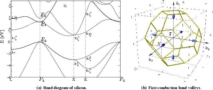
Semiconductor band structures in general and especially for silicon as shown in
Figure 6.4 are hard to describe with an analytical formula.
The plot is
drawn for energy values along particular edges of the irreducible wedge,
cf. Figure 6.3(b). The energy dispersion along
the straight line from point ![]() to point
to point ![]() , which is called
, which is called
![]() -line, is marked by the red line in Figure 6.4(b).
-line, is marked by the red line in Figure 6.4(b).
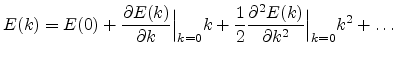
For silicon the conduction band minima lie on the six equivalent
![]() -lines along
-lines along
![]() -directions and occur at about
-directions and occur at about ![]() of the way to the zone
boundary (see Figure 6.4(b)). These are the well-known, equivalent
ellipsoidal constant energy valleys. When electrons gain
of the way to the zone
boundary (see Figure 6.4(b)). These are the well-known, equivalent
ellipsoidal constant energy valleys. When electrons gain
![]() of energy, they can cross the zone boundary.
of energy, they can cross the zone boundary.
There is also a second minimum in the first conduction band at point ![]() , which
lies
, which
lies
![]() about the first valley. The second conduction band valley
is only
about the first valley. The second conduction band valley
is only
![]() above the minimum of the first conduction band.
Carriers above
above the minimum of the first conduction band.
Carriers above
![]() in kinetic energy may reside in either of the two
conduction bands before the second valley of the first band is occupied. Under
large electric fields, electrons
populate the entire Brillouin zone and the band structure at energy minima cannot
be described by simple analytical approximations.
in kinetic energy may reside in either of the two
conduction bands before the second valley of the first band is occupied. Under
large electric fields, electrons
populate the entire Brillouin zone and the band structure at energy minima cannot
be described by simple analytical approximations.
The valence band maximum for the heavy-hole-, light-hole-, and for the
split-off band is located exactly at the ![]() -point (see
Figure 6.4(b)). It is obvious that for a small electric field
the concentration of holes is higher in the region around the
-point (see
Figure 6.4(b)). It is obvious that for a small electric field
the concentration of holes is higher in the region around the
![]() -point. For full band Monte Carlo simulations it is thus important to use a
discretization of the momentum space, which shows a higher mesh density around
the
-point. For full band Monte Carlo simulations it is thus important to use a
discretization of the momentum space, which shows a higher mesh density around
the ![]() -point.
-point.
The complexity of semiconductor band structures forces different approximations
to reduce intricacy and computational costs. Two analytical models, namely
the parabolic and the non-parabolic model are widely used.
The FBMC method produces a more general description, suitable also for higher
energy values. This description is commonly based on the so-called
pseudopotential method. These approximations, especially for valence
bands, are subject of the following section.
A brief review of known analytical band structure approximations is given
to convince the reader and to make this thesis self-contained for later
discussions. An all-embracing description can be found in many basic books
on solid-state physics related to semiconductors such as [112]
and [114].
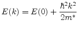
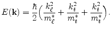
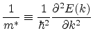
The simplest model of the silicon band structure is based on the effective mass.
If the band structure is known, the energy wave vector relation ![]() in one
dimension can be expanded in a Taylor series as
in one
dimension can be expanded in a Taylor series as
 |
(6.12) |
Generally for diamond crystals such as silicon
(see Figure 6.1) the conduction band has three
minima, one at
![]() (called the
(called the ![]() point), another along
point), another along
![]() directions at the boundary of the first Brillouin zone (called
directions at the boundary of the first Brillouin zone (called
![]() ) and a third one near the zone boundary along
) and a third one near the zone boundary along
![]() directions. cf. Figure 6.4.
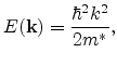
If the first conduction band minimum
directions. cf. Figure 6.4.
If the first conduction band minimum
![]() is described by
is described by
Equation (6.14) describes a band with ellipsoidal constant energy
surfaces. The effective mass is a tensor with different longitudinal and transverse
effective masses,
![]() and
and
![]() , respectively. Material
specific values for
, respectively. Material
specific values for
![]() and
and
![]() can be found
e.g. in [114]. Formula (6.14) is referred to as the
parabolic energy band approximation.
can be found
e.g. in [114]. Formula (6.14) is referred to as the
parabolic energy band approximation.
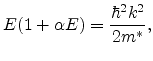
In the case of high applied fields, carriers may be far above the minimum, and the higher order terms in the Taylor series expansion cannot be ignored. For the conduction band, this is approximated by a relation of the form
where ![]() is determined from formula (6.11) at the minimum. For a
minimum at
is determined from formula (6.11) at the minimum. For a
minimum at
![]() ,
,
 |
(6.16) |
where
![]() is the direct bandgap. Formula (6.15) is referred to
as the non-parabolic energy band approximation.
is the direct bandgap. Formula (6.15) is referred to
as the non-parabolic energy band approximation.
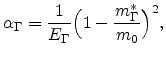
For higher energies, we can approximate
the conduction band with a non parabolic parameter, ![]() , as defined
in Equation (6.15). Nevertheless a non parabolic band
provides a reasonable approximation only up to an energy of about
, as defined
in Equation (6.15). Nevertheless a non parabolic band
provides a reasonable approximation only up to an energy of about
![]() . For example in silicon MOSFETs an important reliability problem
is caused by injection of electrons from the channel into the gate oxide. The
energy barrier at the SiO
. For example in silicon MOSFETs an important reliability problem
is caused by injection of electrons from the channel into the gate oxide. The
energy barrier at the SiO![]() : Si interface is
: Si interface is
![]() . For these
problems simple expressions for
. For these
problems simple expressions for
![]() are not valid any more and a
numerically generated table of
are not valid any more and a
numerically generated table of
![]() must be used.
must be used.
A very useful approach to a numerical evaluation of
![]() is the so
called pseudopotential method [115]. To evaluate
is the so
called pseudopotential method [115]. To evaluate
![]() the Schrödinger equation for the electrons is solved for a bulk semiconductor
in the absence of scattering and without any built-in potential [116].
The pseudopotential method relies on the fact that the band structure is
largely determined by the valence electrons. In addition empirical form factors
have been derived to fit band gaps at the high symmetry
locations. Using this empirical pseudopotential method, the energy band
structures of most common semiconductors have been evaluated and they are
available in tabular form.
the Schrödinger equation for the electrons is solved for a bulk semiconductor
in the absence of scattering and without any built-in potential [116].
The pseudopotential method relies on the fact that the band structure is
largely determined by the valence electrons. In addition empirical form factors
have been derived to fit band gaps at the high symmetry
locations. Using this empirical pseudopotential method, the energy band
structures of most common semiconductors have been evaluated and they are
available in tabular form.