
 |
|
||||
BiographyMarkus Jech was born in Vienna in 1986. He received the degree of Diplomingenieur in Physics from the Technische Universität Wien in 2014. In January 2015 he joined the Institute for Microelectronics, where he is currently working on his doctoral degree. |
|||||
Mixed-Mode Stress in Full {VG, VD} Bias Space
Characterizing the reliability of a technology typically focuses on idealized device degradation regimes, such as bias temperature instability (BTI) and hot-carrier degradation (HCD). Previous studies have characterized the individual degradation modes around their typical worst-case condition within a certain bias space regime. Their interplay within intermediate bias space conditions is often neglected, however, despite its importance in modern complementary metal oxide semiconductor digital circuits. When switching between logic levels, a field-effect transistor experiences a broad range of bias conditions beyond the idealized worst-case bias points.
In order to investigate the degradation characteristics of pMOSFETs in full {VG, VD} bias space from a modeling perspective, we have extended the current 4-state nonradiative multi-phonon (NMP) framework towards non-equilibrium transport dynamics. By explicitly taking non-equilibrium energy distribution functions into account, the impact of a hot-carrier ensemble, as well as secondary generated carriers, on the charging and discharging dynamics of oxide defects can be investigated. In conjunction with our newly developed HCD model, which describes the creation of interface defects due to the interaction of Si-H bonds with energetic carriers, we are able to capture degradation trends in full bias space. In this regard, the modeling framework for HCD is based on a resonance state, which upon electronic relaxation, excites phonon modes of the Si-H complex and eventually triggers dissociation.
The experimental degradation and recovery map over a broad range of VG and VD bias conditions is shown in Fig. 1. The measurement data shows a strong degradation in the mixed-mode, as well as in the HCD, bias regimes, with threshold voltage drifts three times higher than for drift in the BTI region. Additionally, the results suggest a transition from HCD to the mixed-mode region, which is very sensitive to the applied gate bias (see for VD = -2.8 V in Fig. 1). The simulation results for all {VG, VD} combinations are shown in Fig. 2. One can see that the degradation map is in very good agreement with the experimentally extracted values, representing the trends towards the HCD and the mixed-mode regime very well. Moreover, specific features, such as the drift minimum between BTI and mixed-mode conditions, as well as the overall worst-case-conditions at VG = -1.5 V and VD = -2.8 V, are captured well. Furthermore, the recovery behavior is accurately represented, in particular the strong decrease in recovery with increasing drain bias. Such a comprehensive study clearly shows that degradation and recovery dynamics over a broad range of bias conditions can only be adequately described by explicitly considering non-equilibrium effects and their implications for the kinetics of oxide and interface defects.
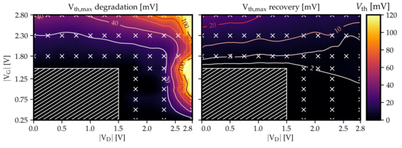
Fig. 1: Experimentally extracted degradation (left) and recovery (right) maps in full bias space outside the operation regime. 55 bias points have been measured, indicated by the crosses.
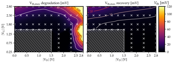
Fig. 2: Simulation results for the bias conditions shown in Fig. 1. The results have been obtained considering the effect of BTI described by oxide defects and the effect of HCD due to the creation of interface states. The general trends, as well as specific features, are captured well by the simulation approach. The maximum degradation is strongly localized in the vicinity of the HCD regime. The damage in the mixed-mode regime is much broader and extends towards the BTI area with a notable drift minimum in between. On the other hand, any significant contribution in the recovery map is only visible for the BTI regime.