
 |
|
||||
BiographyAleksandr Vasilev was born in Republic of Mordovia, Russia in 1990. In 2011 he obtained the Bachelor degree in Electronics and Nanoelectronics from Chuvash State University and the Master degree in Solar Heterostructure Photovoltaics at Saint Petersburg Electrotechnical University "LETI" in Russia in 2013. He joined the Institute for Microelectronics in October 2019, where he is working for the FWF project DEMOS and the CDL for SDS. His research focus will be on defect-centric modeling of reliability issues in SiC devices. |
|||||
Modeling Hysteresis in 4H-SiC MOSFETs
Silicon carbide (SiC), and especially its 4H polytype, has been repeatedly reported as a very promising material for high power electronics. This is because 4H-SiC has a number of unique properties, such as a wide bandgap, a good thermal conductivity, a high saturation velocity and a higher, – when compared to silicon, – breakdown field. Moreover, high power transistors on 4H-SiC have shorter drift zones than those in Si devices with the same on-resistance (Ron).
However, the channel mobility in SiC devices is substantially lower than the bulk mobility. This behavior is related to a significant concentration of defects in the vicinity of the SiC/SiO2 interface. A related reliability concern in that regard is that the threshold voltage shifts, Vth, observed in SiC devices subjected to positive/negative gate bias stress are typically higher than the drifts of ΔVth in Si-based metal-oxide-semiconductor devices. Therefore, one can conclude that the concentration of defects at the SiC/SiO2 interface is substantially higher than the defect density in the bulk. These near-interface defects are also responsible for other detrimental phenomena, such as the hysteresis of the current-voltage characteristics, bias temperature instability and also hot-carrier degradation.
In Fig. 1, a set of Id-Vgs characteristics (here Id is the drain current and Vgs is the gate voltage) measured over a wide temperature range are shown. One can see that the curves measured with the gate voltage sweeping up and down are shifted with respect to each other, which becomes more pronounced at lower temperatures. On top of this trend, one can also see that the threshold voltage shifts towards lower values at elevated temperatures.
To describe and model these effects, we employ the nonradiative multi-phonon (NMP) model implemented in the device and circuit simulator, MinimosNT, used within the GTS framework. Note that although the full NMP model considers four states of the defects, the compact two-state form of the model also enables one to explain the majority of the charge trapping phenomena at significantly reduced computational effort. The two-state model takes into account the neutral (precursor) and the charged (defect) states; the corresponding barriers for transitions between these states determine the rates of the capture and emission reactions. The difference in the cumulative charge captured by the traps at sweeping-up and the charge emitted during sweeping-down determines the width of the hysteresis (see Fig. 1). Fig. 2 shows good agreement between experimental and simulated transfer characteristics obtained at T = 142 K. One can see that among other things, our simulation framework can reproduce the hysteresis width of 0.23 V with good accuracy.
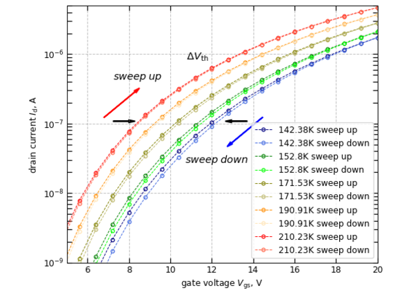
Fig. 1: A series of Id-Vgs curves measured over a wide temperature range of 140-210 K. The characteristics obtained at Vgs sweeping-up and down are shifted with respect to each other. This effect is called "hysteresis" and becomes more pronounced at lower temperatures.
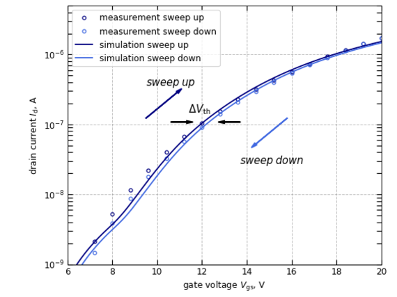
Fig. 2: Simulated versus measured Id-Vgs curves for T = 142 K. One can see that our modeling framework can represent the hysteresis with good accuracy.