
 |
|
||||
BiographyDominic Waldhör was born in Linz, Austria in 1992. He studied at the TU Wien, Vienna, Austria where he received the BSc degree in Electrical Engineering and the Diplomingenieur degree in Microelectronics and Photonics in 2018. He joined the Institute for Microelectronics in October 2018 where he works as PhD student. His current research focuses on the ab initio simulation of oxide defects in semiconductor devices. |
|||||
Ab-Initio Treatment of Defect-Strain Interaction in Amorphous SiO2
Silicon dioxide (SiO2) is widely used as a gate oxide in silicon-based electronics. However, hole trapping by defects in the SiO2 layer gives rise to major reliability challenges, like bias temperature instability or random telegraph noise in modern metal-oxide-semiconductor devices. To investigate these effects, dedicated measurement tools and characterization techniques have been developed. In order to study the underlying physical processes of these phenomena on an atomistic level, density functional theory (DFT) simulations are performed.
The oxide layer near the device channel interface is inherently strained due to the lattice mismatch between the Si and SiO2. This mechanical stress alters the atomic structure, in particular Si-O bond lengths, and thus can potentially change the electrical behavior of oxide defects. In previous theoretical defect studies, such structural distortions have been neglected, but they can be of significant importance for the understanding of the charge trapping kinetics of the defects. Our work utilizes DFT in order to study the impact of mechanical stress in the oxide on the behavior of promising hole trap candidates, like the Hydroxyl-E’ center shown in Fig. 1. Applying an external compressive stress to the atomistic SiO2 structure leads to a systematic increase in the corresponding charge trap levels as depicted in Fig. 2. Depending on the initial position of the trap level with respect to the Si valence band, this shift can lead to increased hole trapping rates. If the defect level is pushed inside the Si bandgap, however, the defect becomes a fixed positive charge. The strong defect-stress interaction of the Hydroxyl-E’ center stems from the pronounced dependence of the defect formation energy on the Si-O bond length at the defect site (see Fig. 3), which is sensitive to the local mechanical stress.
Our findings also suggest that defects are more likely to form at elongated Si-O bonds due to the lower formation energy at these sites. This supports experimental evidence for larger defect densities near the Si/SiO2 interface as compared to the SiO2 bulk due to the presence of strained bonds in this region. Furthermore, our study indicates that only slight changes in the local defect environment can significantly alter the hole trapping rate and thus macroscopic device degradation.
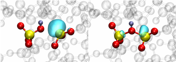
Fig. 1: Hydroxyl-E' center in the neutral state (left) and after trapping a hole (right) in amorphous SiO2.
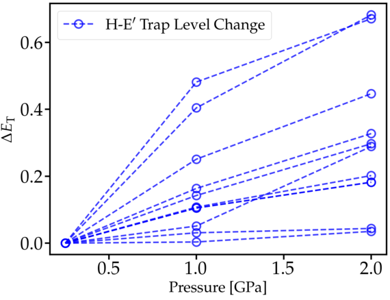
Fig. 2: Trap level shift as a function of applied stress for multiple Hydroxyl-E' centers. The trap level increases systematically with mechanical stress.
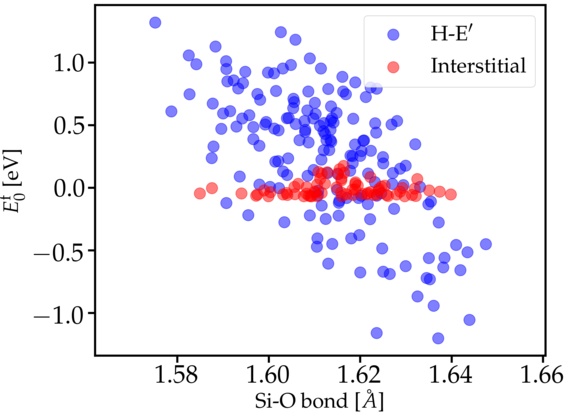
Fig. 3: Hydroxyl-E' formation energy at multiple sites with varying Si-O bond lengths. There is a clear correlation between the bond length and the stability of the defect.