
 |
|
||||
BiographyMarkus Jech was born in Vienna in 1986. He received the degree of Diplomingenieur in Physics from the Technische Universität Wien in 2014. In January 2015 he joined the Institute for Microelectronics, where he is currently working on his doctoral degree. |
|||||
Structural and Electronic Properties of Pb-Centers
Point defects are unavoidable in micro- and nano-electronic devices and impose limits on their reliability. In particular, structural disorder at material interfaces, such as the Si/SiO2 system, provokes an increased number of electrically active defects. Using electron-spin-resonance (ESR) spectroscopy, two detrimental types, referred to as Pb-centers, have been clearly identified on the most industrially relevant <100> surface, called Pb0 and Pb1. The dominant Pb0-center has been experimentally identified as a trivalent interfacial silicon atom back-bonded to three other Si atoms in the bulk lattice. On the other hand, the structural properties of the Pb1-center are still controversial, and speculations range from a distorted Pb0-center to a a silicon dangling bond (DB) back-bonded to oxygen atoms of the SiO2 network.
Using first-principles approaches, we can shed light on the atomic structure of the various defects at the Si/SiO2 interface by unequivocally matching our calculations to their experimental ESR response. By generating a number of Si/SiO2 interface models, we explore the various structural and chemical environments of an interfacial silicon DB. One example of an interfacial Si DB in its realistic three-dimensional environment is shown in Fig. 1. The defect orbital is fully localized on the central silicon atom, and the trivalent Si DB perfectly resembles the structural properties of the well-known Pb0-center mentioned above. Subsequently, we calculated its g matrix and the corresponding hyperfine parameters, allowing us to reconstruct the defects' ESR spectrum (see Fig. 2). Its g matrix shows an almost perfect axial symmetry (g1 = 2.001, g2 = g3 = 2.01) with the symmetry axis being the <111> direction as indicated in Fig. 2. The calculated ESR spectrum matches the measurement results very well (see Fig. 2), exhibiting the main sharp peak at around 3400 G, with two additional symmetric side peaks due to the natural abundance of silicon.
Ultimately, these ab initio based modeling approaches offer new insight into the fundamental properties of defect structures and improve our current understanding of their structural and electronic characteristics.
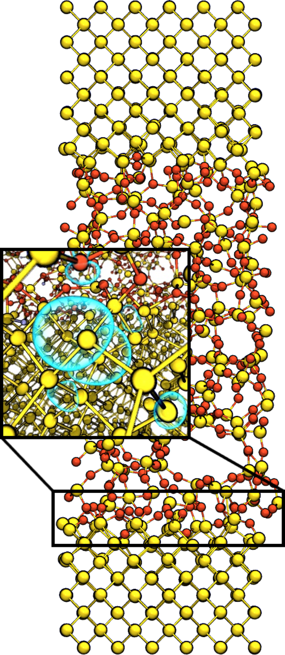
Fig. 1: A realistic Si/SiO2 model with one interface defect, a silicon DB, known as a Pb-center.
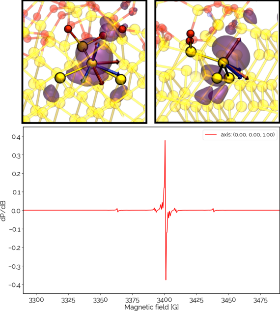
Fig. 2: The defect orbital, together with its symmetry, axis and the calculated ESR spectrum.