
 |
|
||||
BiographyHans Kosina received the Diplomingenieur degree in electrical engineering and PhD from the Technische Universität Wien in 1987 and 1992, respectively. He was with the Institute of Flexible Automation at the Technische Universität Wien for one year and then joined the Institute for Microelectronics, where he is currently an associate professor. He received the venia docendi in microelectronics in 1998. In the summer of 1993, he was a visiting scientist at Motorola Inc., Austin, Texas, and in the summer of 1999, a visiting scientist at Intel Corp., Santa Clara, California. Dr. Kosina was chairman of the ''11th International Workshop on Computational Electronics'' held in Vienna in May 2006 and is a member of the advisory board of the International Workshop on Computational Nanotechnology. He has served as an Associate Editor of the IEEE Transactions on Computer-Aided Design of Circuits and Systems and the Journal of Computational Electronics. His current research interests include nanoelectronic device modeling and the development of numerical methods and algorithms for classical and quantum transport calculations. |
|||||
Numerical Modeling of Nanostructured Semiconductor Devices
A project on negative capacitance and ferroelectric devices has been completed. Several models and simulators have been developed to present a landscape of simulation options for the investigation and design of ferroelectric devices depending on the priorities and intent of a modeling investigation. The two main outcomes of this project are the creation of a ferroelectric physics module of Python codes for the TCAD framework of our cooperation partner, GTS, and a more compact simulator of ferroelectric transistors, ComphyFE, which builds upon the pre-existing code-base Comphy. The TCAD framework models allow for full 3D simulation and the study of real polycrystalline ferroelectric films, with true spatially defined grains, where ComphyFE allows straightforward modeling of the competing effects of ferroelectric switching and charge-trapping on the performance and behavior of FeFETs.
A project on numerical methods for the stationary Wigner equation and the von Neumann equation has entered its second year. The stationary Wigner equation has a singularity at zero momentum (k = 0). In order to get a non-singular solution, we impose a constraint on the solution at k = 0. We investigated two solution strategies for the constrained von Neumann equation. The first is based on the finite difference method and solves the equation in a least-squares sense. The second is a Petrov-Galerkin method with sine and cosine ansatz functions. The constraint in the Wigner equation is interpreted as an extra test function and is naturally incorporated into the method. We also incorporate a complex absorbing potential in order to diminish unphysical reflections of outgoing waves. Both methods were evaluated by simulating a resonant tunneling diode and via comparison with the quantum transmitting boundary method (QTBM). The numerical capability of the methods is demonstrated by simulating up to a high bias that is beyond the usual operating conditions of the device. The QTBM and the Wigner function model fit almost perfectly up to a bias of 2 V. In order to achieve high accuracy, a coherence length of at least 60 nm must be assumed, and a fine mesh has to be used for the simulation.
A new project has started that analyzes different quantum transport models with respect to their applicability to emerging technologies and their usability in device TCAD. The numerical aspects associated with each model are also considered. The project aims to identify the transport model that represents a good trade off between physical accuracy and computational demand. As a test case, we considered nanoribbons of MoS2 in the 1T' phase, which is a topological insulator. A Newton-solver for calculating the transverse modes and the subband structure has been developed. The band gap can be controlled by a vertical electric field (Fig 1. and Fig. 2). We developed a direct method for the calculation of the surface Green's function, which is computationally more efficient than the widely used iterative method due to Sancho and Rubio.
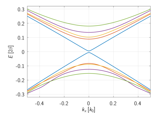
Fig. 1: Subband structure of a 28.86 nm wide nanoribbon at zero vertical electrical field. The subbands with a nearly linear dispersion correspond to the topologically protected edge states.
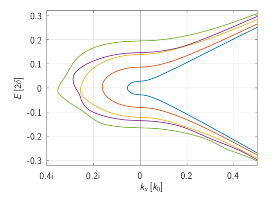
Fig. 2: Complex subband structure of the nanoribbon at the characteristic vertical field at which the bandgap in the bulk material would close.