
 |
|
||||
BiographyAleksandr Vasilev was born in Republic of Mordovia, Russia in 1990. In 2011 he obtained the Bachelor degree in Electronics and Nanoelectronics from Chuvash State University and the Master degree in Solar Heterostructure Photovoltaics at Saint Petersburg Electrotechnical University "LETI" in Russia in 2013. He joined the Institute for Microelectronics in October 2019, where he is working for the FWF project DEMOS and the CDL for SDS. His research focus will be on defect-centric modeling of reliability issues in SiC devices. |
|||||
Modeling the Hysteresis of Current-Voltage Characteristics in Planar 4H-SiC MOSFETs
Even though silicon carbide (4H-SiC) is an appropriate material for high-voltage and high frequency electronics, its application in MOSFETs leads to some technological and physical challenges. In particular, electrically active defects located at the 4H-SiC/SiO2 interface and bulk oxide (SiO2) can alter the device characteristics and thus affect their overall performance. Such so-called border traps, which are typically modeled to be randomly distributed up to 2 nm away from the interface, can lead to a significant drift of the threshold voltage of the device. Furthermore, these defects give rise to a hysteresis of the current-voltage, Id-Vgs, characteristics when up and down sweeps of the gate voltage are measured. To understand this behavior, a physics-based modeling approach that considers the trapping kinetics of border states has been developed.
One can see from our measurements, which were conducted at temperatures between 150 K and 300 K, that the transfer characteristics shift towards higher gate voltages when the gate bias is swept downwards. This differs in comparison to the curves where upward sweeps of the gate bias are applied. The hysteresis arising from these sweeps becomes more pronounced at lower temperatures. It can also be observed that the threshold voltage shifts by 6 V towards higher gate biases when the temperature decreases (see Fig. 1).
To explain the observed hysteresis behavior, we assume that acceptor-like traps with charge transition level 0/-1 and a trap energy level near the 4H-SiC conduction band are responsible for this trend. To prove our assumption, we simulated the device characteristics using our TCAD simulator and employed a two-state non-radiative multiphonon model (NMP) for investigating the effect of charge trapping. By changing the fundamental NMP parameters, we fit the forward and backward barriers, which correspond to capture and emission times, and the trap concentration to replicate experimental transfer characteristics.
Due to the considerable amount of acceptor-like traps, which cause a significant positive shift of the threshold voltage, we added a donor-like trap-band to compensate for this shift. The capture and emission times of the defects depend on temperature and become shorter at elevated temperatures. Finally, our simulation results nicely explain the hysteresis width vs. temperature (see Fig. 2), indicating the high accuracy of our simulation models.
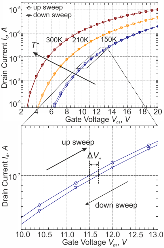
Fig. 1: A series of Id-Vgs curves measured at 150 K, 210 K and 300 K. The hysteresis was obtained as the difference between the curves sweeping down and up at a reference drain current of 10-7 A.

Fig. 2: Simulated vs. measured hysteresis over a wide temperature range.