
 |
|
||||
BiographyHajdin Ceric was born in Sarajevo, Bosnia and Herzegovina, in 1970. He studied electrical engineering at the Electrotechnical Faculty of the University of Sarajevo and the Technische Universität Wien, where he received the degree of Diplomingenieur in 2000. In 2005 he received his PhD in technical sciences and in 2015 his venia docendi in microelectronics from the Technische Universität Wien. In 2010 he was appointed the head of the Christian Doppler Laboratory for Reliability Issues in Microelectronics. He is currently an Associate Professor at the Institute for Microelectronics. His research interests include modeling and simulation of reliability issues in interconnects for ultra large-scale integration. |
|||||
Impact of Microstructure on Gold Interconnect Reliability
In contrast to the plethora of electromigration studies which have been performed on both aluminum and copper metallization systems for silicon-based semiconductors, the number of electromigration studies on passivated gold electroplated metallization systems for III-V based semiconductor devices is very limited. Compound semiconductor devices, such as metal semiconductor field effect transistors (MESFETs) and heterojunction bipolar transistors (HBTs) in high-power applications, exclusively use gold films for interconnects and contacts. Gold is the metal of choice for interconnects implemented on GaAs, because it forms a very low-resistance ohmic contact, has a high melting temperature, and has a low resistivity. Crucial segments of gold metallization used for GaAs devices are susceptible to significant electromigration degradation and have a microstructure with a thousands of grains. Simulating the influence of microstructure on the electromigration reliability of a metallic interconnect is a challenging task due to the complexity of grain boundary physics and due to the large number of grains. In our work, a novel approach for the numerically efficient simulation of an interconnect containing thousands of grains is introduced. A number of grains are grouped into larger grain compounds, and a detailed grain boundary model is applied at the boundaries of these domains. The boundaries of the large grain compounds are chosen to comprise characteristic segments of the interconnect geometry, e.g., vias. Alternatively, these segments can also be divided into several grain compounds. The size statistics of grain compounds are set according to the experimentally obtained statistics of grain size distribution. Inside the compounds, the effective diffusivity is calculated as a weighted sum of contributions from the grain bulk and from the grain boundaries. An example of the generated microstructure used for simulations is presented in Fig. 1. The microstructure modeling is integrated in the usual modeling framework for simulation of electromigration reliability, which comprises the solution of the vacancy balance equation together with the Laplace equation, the heat-transport equation, and the mechanical equations. The simulation provides as output, for an arbitrary three-dimensional multilayer interconnect geometry and for given initial and boundary conditions: the temperature distribution, the current density distribution, the tensorial mechanical stress field, and the point defect (vacancy) distribution. These values enable the determination of the interconnect lifetime. All simulations are performed with COMSOL multiphysics and the background gold microstructure is generated using NEPER, a software package for polycrystal generation and meshing. An example of interconnect segment with grain boundaries is presented in Fig. 2.
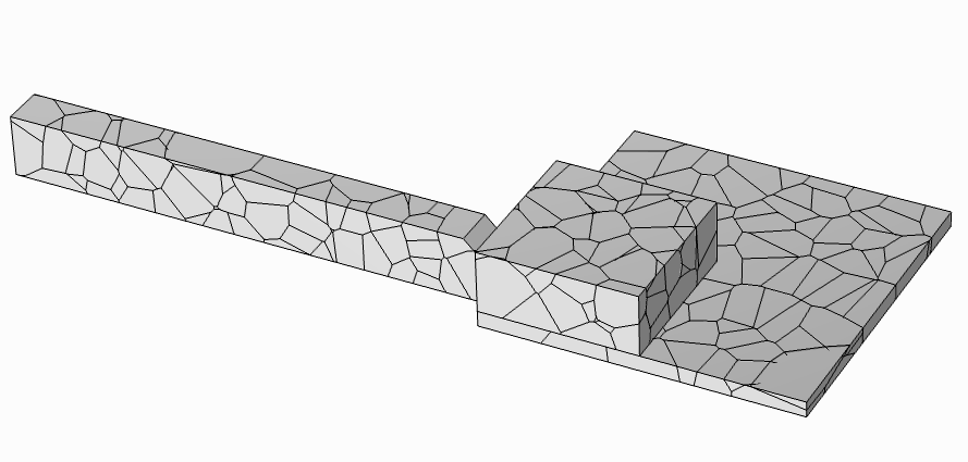
Fig. 1: Segment of gold interconnect with microstructure used for simulation.
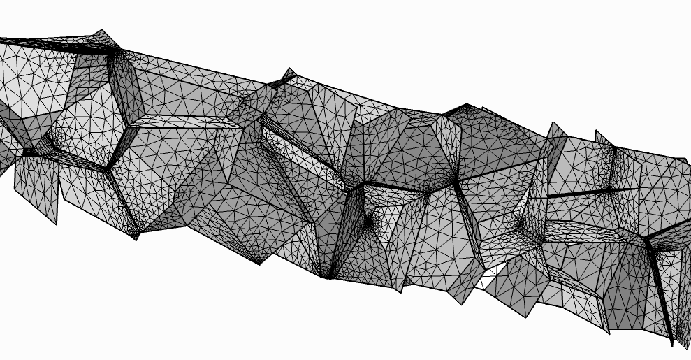
Fig. 2: Grain boundaries used for simulative studies of gold interconnect reliability meshed with a fine finite element mesh.