
 |
|
||||
BiographyAl-Moatasem El-Sayed was born in Sheffield, United Kingdom in 1988. He completed his Masters in chemistry at the University of Manchester in 2010. He went on to do his Ph.D in physics at University College, London, focussing on atomistic modeling of point defects in oxides. He then joined the Institute of Microelectronics in June 2015, his current research interests are modeling of point defects in oxides and their effect on electronic devices. |
|||||
Atomistic Modeling of Electronic Device Phenomena
Materials modeling has become an increasingly accurate and invaluable tool to characterize and predict material properties. Over the past few decades, it has been increasingly applied to issues related to electronic devices and their reliability. Our work focuses on electronic device issues at the atomic scale. We therefore apply a wide range of atomistic modeling techniques to various novel materials and combinations used in electronic devices.
A particularly prominent issue is the role of point defects on electronic device reliability issues. They have long been implicated in a wide range of reliability and stability issues. In fact, the Si-based electronic devices we see today are due to the low defect density between Si and its native oxide. Such a low defect density is extremely desirable and very difficult to achieve in other material combinations.
One example of a more novel material system that we have been working on is the SiGe system. This material system has been chosen due to the higher carrier mobility in Ge, which is somewhat preserved in the SiGe alloy. Devices using SiGe can be fabricated in various configurations, from planar to more exotic nanowire transistors. Typically, the bulk substrate is composed of Si, while the channel layer is mostly composed of SiGe. The dielectric layer is typically made of thermally grown silicon dioxide, as is the case for Si devices. However, the dielectric layer typically contains substitutional Ge dispersed throughout the material.
In order to understand the role of point defects in SiGe devices, we have simulated the well-known oxygen vacancy in SiGeO2, with varying concentrations of Ge from 0% to 100%. We found that the relaxation behavior of the vacancy was similar across all concentrations, and was able to trap either an electron or hole. Fig. 1 shows an example of a positively charged state in two different configurations. The chemical environment of the defect was found to play a very large role in a property known as the charge transition level. This effectively determines the Fermi level at which a charge transition takes place in an electronic device. Due to the wide range of charge transition levels caused by the varying chemical environment of the defect, the oxygen vacancy could potentially play a role in device reliability issues, in contrast to the same defect in pure silicon dioxide.
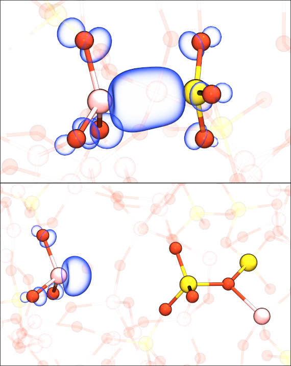
Fig. 1: Two configurations of the positively charged vacancy in SiGeO2