
 |
|
||||
BiographyYury Illarionov was born in Leningrad (now Saint-Petersburg) in 1988. He studied solid state physics at the Physical Science and Technology Faculty of St. Petersburg State Polytechnical University where he received the B.Sc. and M.Sc. degrees in 2009 and 2011, respectively. From 2010 to 2012 he studied advanced material science in Grenoble Institute of Technology (France) and University of Augsburg (Germany) in frameworks of Functionalized Advanced Materials and Engineering (FAME) Erasmus Mundus program and in September 2012 received a double European M.Sc. degree. His scientific carrier has started in October 2007 in Ioffe Physical-Technical Institute (Russia) and in November 2011 he joined the PhD program there. He also visited IRCELYON (France, May-July 2011) and Singapore Institute of Manufacturing Technology (Singapore, February-July 2012) as a young guest researcher. He joined the Institute for Microelectronics in February 2013. In January 2015 he received the PhD degree in semiconductor physics from Ioffe Physical-Technical Institute and in December 2015 the Dr.techn. degree from TU Wien. Since January 2016 Dr. Yury Illarionov is a postdoc researcher working on reliability of the next-generation 2D FETs with graphene, MoS2 and phosphorene. |
|||||
Fabrication and Variability Analysis of CVD-GFETs with Record-thin CaF2 Insulators
Graphene is a promising material with numerous properties that can be exploited in optoelectronics and sensors. Many of these devices require high-quality insulators to either form graphene FETs (GFETs) or otherwise protect graphene. Previously used amorphous oxides contain numerous border traps which cause severe hysteresis and long-term drifts of the gate transfer characteristics. As a promising alternative, we have demonstrated GFETs with 2 nm thick CaF2 insulators previously used in the most stable MoS2 FETs reported so far. CaF2 is an ionic crystal insulator with good dielectric properties (ε = 8.43, EG = 12.1 eV) which forms quasi van der Waals interfaces with 2D materials. We have fabricated >100 single-layer GFETs on Si/CaF2 substrates (Fig. 1a) prepared by our established molecular beam epitaxy method at 250
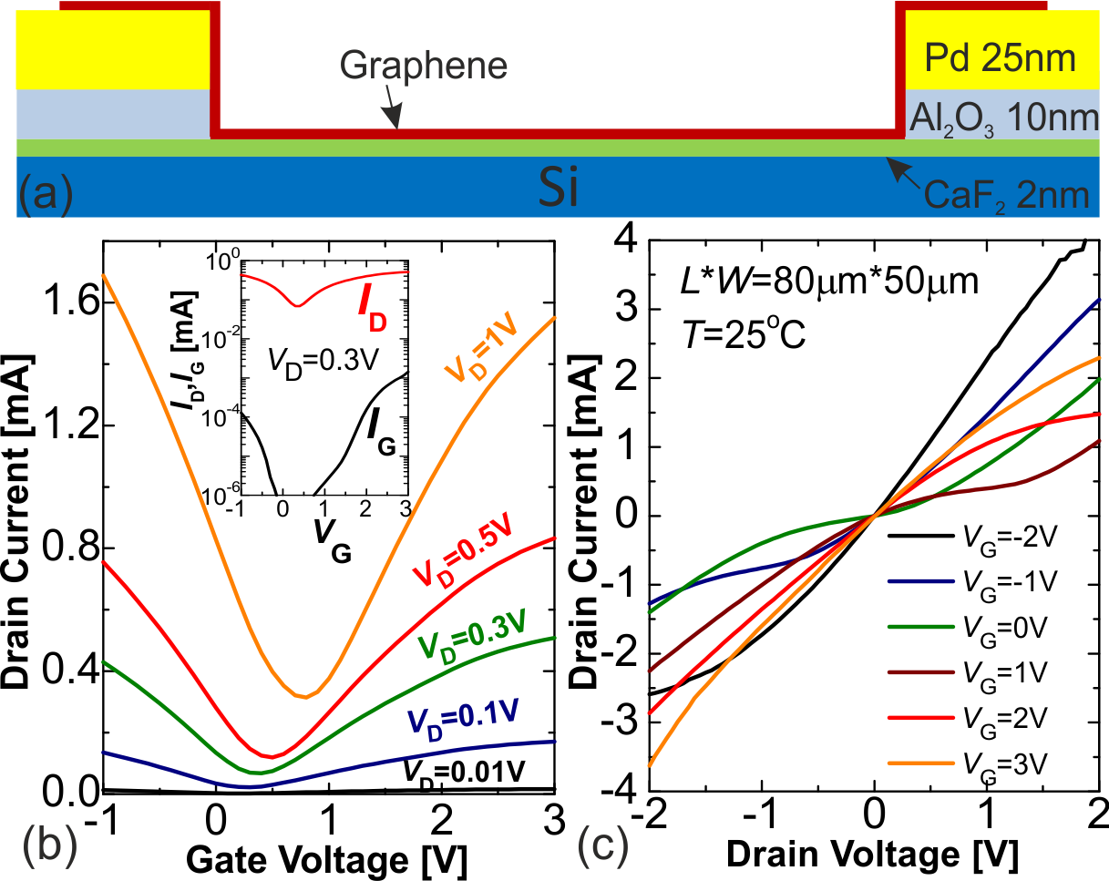
Fig. 1: (a) Schematic structure of our back-gated GFETs with 2 nm CaF2 insulators. (b) Typical ID-VG characteristics of these devices. The inset shows that the gate leakage current through our thin CaF2 layers is small compared to the drain current. (c) The ID-VD characteristics measured for the same GFET exhibit some ambipolar kinks.
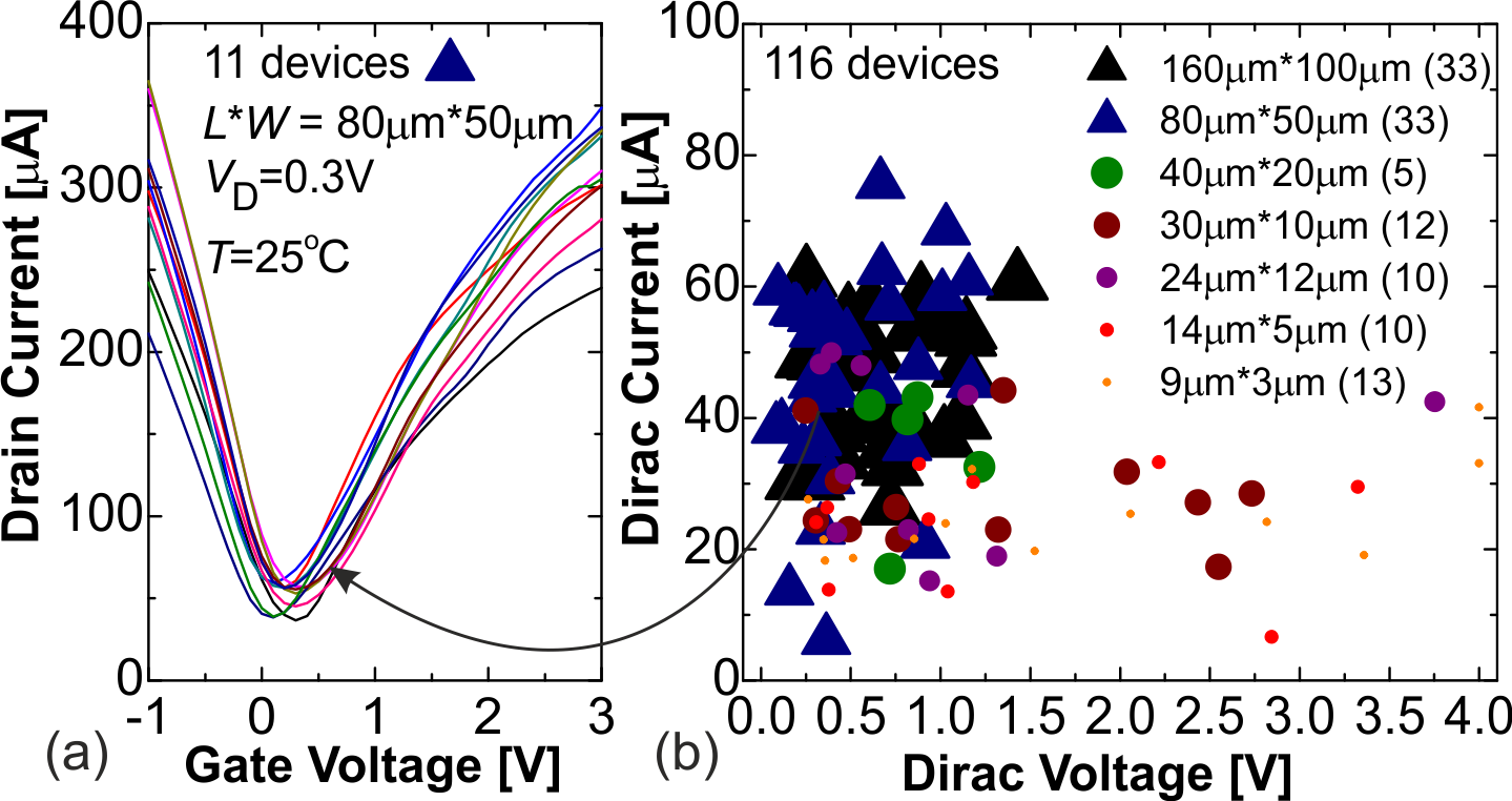
Fig. 2: (a) ID-VG characteristics of 11 similar GFETs with 80µm×50µm channels selected from our total statistics of 116 devices with different channel dimensions. (b) The distribution of IDirac vs. VDirac for all 116 devices; the number of devices with the corresponding channel dimension is marked in brackets in the legend. The measurements have been done before any annealing step, and some smaller devices have a more positive VDirac (for those GFETs we used a VG sweep range from 0 to 4V).