
 |
|
||||
BiographyXaver Klemenschits was born in Vienna in 1994. He studied Nanoscale Physics at the University of Birmingham, England, for which he received the degree of MSc in 2017. He joined the Institute for Microelectronics in August 2017, where he is working on topography simulation using different deposition and etching models. |
|||||
A Geometric Advection Algorithm for the Emulation of Microelectronic Fabrication
Process technology computer aided design (TCAD) is essential in order to simulate the complex fabrication of advanced microelectronic structures. Due to demands of high efficiency and simplicity, process emulation techniques have become more important than ever before. These describe the effect of a fabrication step using only the geometric properties, gathered from experimental data or the results of physical simulations.
Traditional emulation algorithms are, however, strongly limited in their accuracy due to their reliance on explicit surface representations, while traditional simulation techniques, such as the level set (LS) method, are inefficient and suffer from numerical limitations.
In order to combine the advantages of the level set method — namely, robust merger and separation of material — with the efficiency of explicit methods, a geometric advection algorithm for the emulation of microelectronic fabrication processes has been developed [1]. Starting from an explicit surface, a geometric advection distribution is placed at every point on the initial surface to generate the final surface, as shown in Fig. 1. The level set values of the final surface are then calculated for every grid point on the level set, resulting in a valid final level set, as shown in Fig. 1 [2]. The robustness of the final surface description is guaranteed, as the LS automatically deals with potentially complex surface deformations. Additionally, since calculations are performed directly in the level set, no costly conversions to explicit surfaces are required, as the initial surface points can be generated cheaply from the LS grid.
The applicability to the emulation of modern semiconductor manufacture was shown on several high-aspect-ratio structures, as seen in Fig. 3. Since there are no strong limitations on the shape of a geometric distribution or the type of process which can be modeled, this new algorithm presents a promising alternative to traditional methods, combining the performance of explicit methods and the robustness of implicit surface descriptions.
[1] https://doi.org/10.23919/SISPAD49475.2020.9241678 [2] https://doi.org/10.1016/j.cma.2021.114196 [3] https://doi.org/10.1016/j.mee.2018.01.034
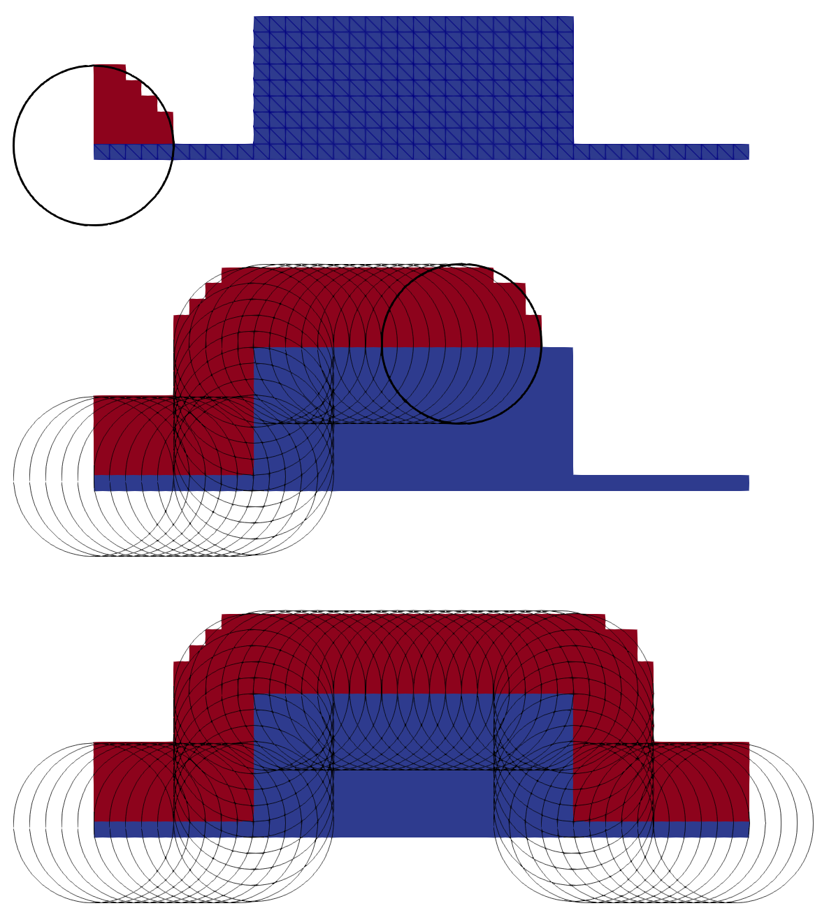
Fig. 1: Schematic representation of the idea behind geometric advection. A geometric advection distribution (black circle) is centered at every point on the initial surface and filled with new material (red) to be deposited on the substrate (blue). By combining all distributions, a robust description of the final surface is achieved.
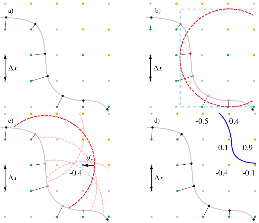
Fig. 2: Visualization of the algorithm in the level set. a) Generate explicit surface points (black) from LS grid points (green). Identify potential final surface points (orange) and pick the first for which the LS value has not been calculated, the candidate point. b) Identify points (pink) which could set the value of the current candidate point. c) Calculate the LS value for all pink points and choose the lowest one as the final LS value. d) Once all LS values of orange points have been computed, the new LS is complete.
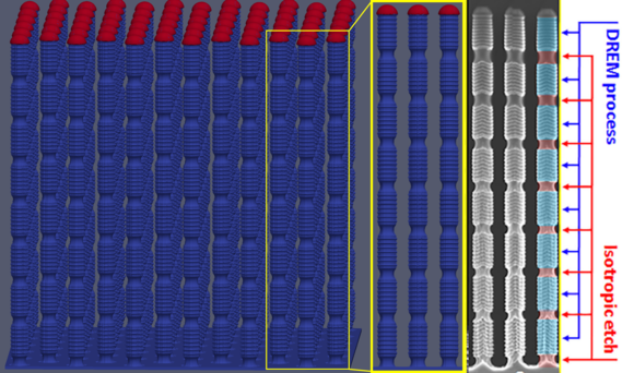
Fig. 3: The applicability to real processes has been shown by simulating a sausage chain structure in 3D using a cyclic etch and deposition technique [3].