
 |
|
||||
BiographyTheresia Knobloch is a postdoctoral researcher focusing on fabrication, experimental characterization, and physical modeling of nanoelectronic devices based on 2D materials. She obtained her doctoral degree from TU Wien in 2021 and performed parts of her Ph.D. research as a visiting scholar at Purdue University, USA in 2018 and 2019 and Soochow University, China in 2017. For her work, she received several awards including the IEEE EDS Ph.D. Student Fellowship in 2021 and the Best Student Paper Award at the DRC in 2020. She joined the Institue for Microelectronics in 2016 while completing her master's degree in microelectronics and photonics. She acquired both her M.Sc. in 2016 and her B.Sc. in technical physics in 2014 from TU Wien with distinction. Currently, she primarily studies the electrical stability and reliability of 2D material-based field-effect transistors. |
|||||
Suitable Gate Insulators for Reliable 2D Nanoelectronics
In general, performance gains of advanced semiconductor technology nodes are realized via increases in the complexity of the system architecture on all levels. At the device level, stacked nanosheet field-effect transistor (FET) designs are currently being explored by leading semiconductor manufacturers. While these nanosheet devices still rely, at present, on silicon channels, further scaling of the channel length requires shrinking of the channel thickness. However, at the required thickness of few nanometers, the mobility in silicon decreases dramatically, whereas in two-dimensional (2D) semiconductors, sizable mobilities are maintained at atomic-layer thicknesses below one nanometer. Despite the promises 2D semiconductors hold for future technology nodes, major challenges remain, such as the identification of suitable gate insulators. Good gate insulators for 2D semiconductor-based FETs should provide a high-quality interface and a minimum number of electrically active border traps while being scalable down to small insulator thicknesses.
Due to its wide availability, many prototype devices so far have used silicon dioxide (SiO2) as a gate insulator. In Fig. 1, the atomic structure of the interface between SiO2 and the layered 2D semiconductor molybdenum disulfide (MoS2) is shown. While, in the ideal case, the surface of MoS2 is a defect-free Van der Waals surface, the surface of amorphous SiO2 intrinsically shows a high density of defects and dangling bonds. In 2D FETs, these two surfaces form the critical oxide to semiconductor interface, which for the example of SiO2/MoS2 suffers from high interface trap densities on the order of 1013cm-2. This interface trap density exceeds the requirements for industrial applications by about two orders of magnitude, and thereby degrades the observed semiconductor mobility and sub-threshold swing. Moreover, charge trapping of electrons at charge traps in the SiO2 causes large drifts of the threshold voltage. As the conduction band edge of MoS2 is aligned within the electron trapping band of SiO2, charge trapping events are frequent. Therefore, the threshold voltage shifts for negative bias temperature instability (NBTI) measurements on MoS2/SiO2 FETs, when normalized by the effective gate stress field of 9.75MV/cm, are around two orders of magnitude higher than the shifts for commercial Si/SiO2 FETs, see Fig. 2.
In summary, SiO2 is not a suitable gate insulator for 2D FETs, and the search for suitable gate insulators for 2D nanoelectronics continues to be an ongoing research effort. Promising candidates currently being explored include layered insulators, (e.g., muscovite mica), ionic fluorides (e.g., calcium fluoride), or native oxides to layered semiconductors (e.g., hafnium dioxide or bismuth selenide).

Fig. 1: Illustration of the atomic structure of the MoS2/SiO2 interface which contains many dangling bonds, resulting in a defective interface. Here, molybdenum atoms are shown in black, sulfur in light yellow, silicon in dark yellow, oxygen in red, and hydrogen in blue.
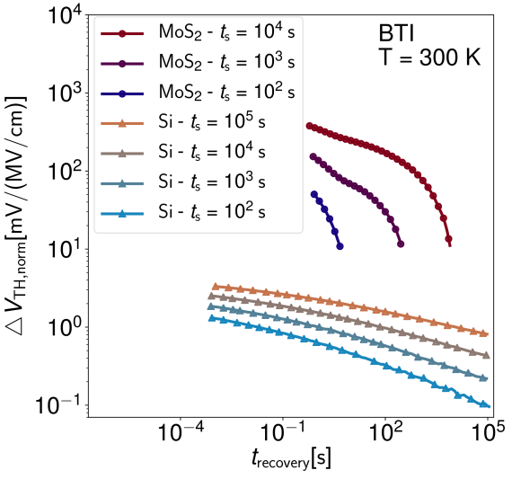
Fig. 2: Negative bias temperature instability (NBTI) as measured on silicon/siliconoxynitride and MoS2/ silicon dioxide FETs. BTI shifts are normalized by the respective gate oxide stress fields to ensure comparability.