
 |
|
||||
BiographyChristoph Lenz was born in 1988 in Vienna, Austria. He studied Technical Mathematics at the Technische Universität Wien where he received his Bachelor's degree (2017) and the degree of Diplomingenieur (2019). After finishing his thesis which was written in collaboration with the IuE, he decided to join the research team of the institute, where he is currently working on his doctoral degree. His research interests include high performance algorithms and data structures and he is working within the scope of the Christian Doppler Laboratory for High Performance TCAD. |
|||||
Curvature-based Feature Detection for Hierarchical Grid Refinement in TCAD Topography Simulations
Many non-planar semiconductor device geometries (e.g., FinFETs) are fabricated by employing strongly anisotropic processing techniques. One of those techniques is selective epitaxial growth (SEG), which is characterized by crystal facets. The resulting wafer topographies contain high curvatures and essentially flat areas. Consequently, the underlying grids need to offer high resolutions to accurately resolve the high-curvature features and the material interfaces during a process simulation, while keeping the overall run time as small as possible to maximize practicability. This is achieved by employing hierarchical grids consisting of a base grid spanning the entire simulation domain, and sub-grids with a higher resolution around points of interest (e.g., features). Fig. 1 shows an illustration of the surface of a SiGe crystal represented by a level-set function on a base grid and three sub-grids (blue) with a two-times higher resolution.
The features of the wafer surface are detected by calculating the curvature κ of the wafer surface and a user-supplied threshold parameter C. After all features of the wafer surface have been detected, an automatic mesh placement algorithm is used to optimally position sub-grids so that all features are efficiently covered.
The applicability of this approach is demonstrated by simulating an SEG process, where SiGe fins are grown inside a SiO2 trench. The SEG process consists of 47 cyclic SEG steps, abstracted to a continuous process. This process has been simulated with three different grid parameters: Coarse consists of a single grid with a base resolution of 0.002 μm, Fine also consists of a single grid with a base resolution of 0.0005 μm, and Multi-grid consists of a base grid with a resolution of 0.002 μm and several sub-grids with a resolution of 0.0005 μm. Fig. 2 shows the surface of the SiGe crystal after the final simulation time step simulated with all three grid parameters.
The results from the Fine and Multi-grid simulation agree with one another. However, the simulation run with the Coarse grid parameters shows that this grid resolution is not sufficient to properly represent the peak of the SiGe crystal. Multi-grid enables a 32% faster simulation time while maintaining the accuracy of the simulation run with the Fine grid-parameters. Fig. 3 shows the positioned sub-grids after 24 SEG cycles.
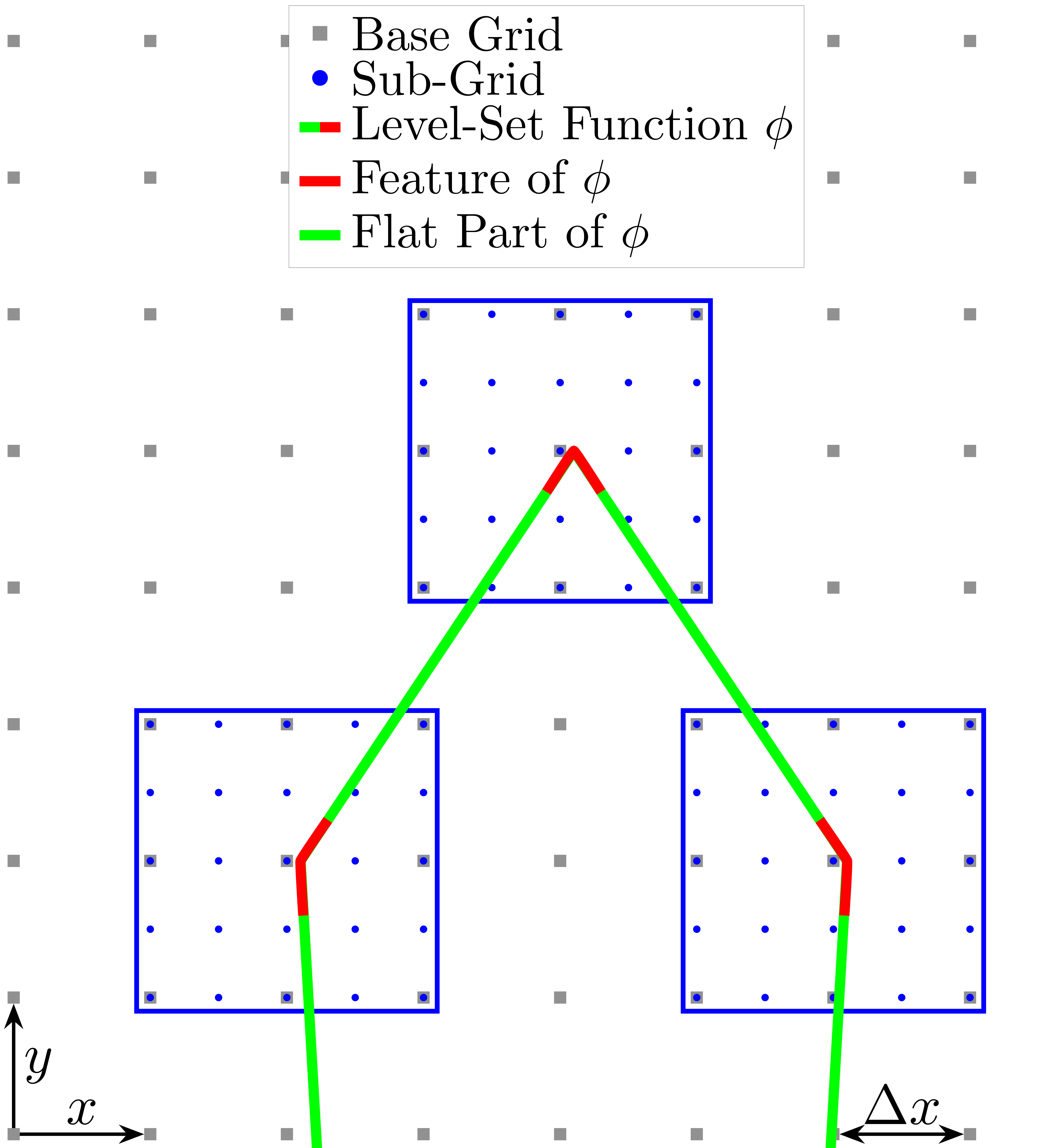
Fig. 1: Illustration of a level-set function φ (green/red line segments) with three features (i.e., corners; red line segments) on a hierarchical grid. The base grid has a resolution of Δx, and the features of φ are covered by sub-grids with a two-times higher resolution (blue boxes).
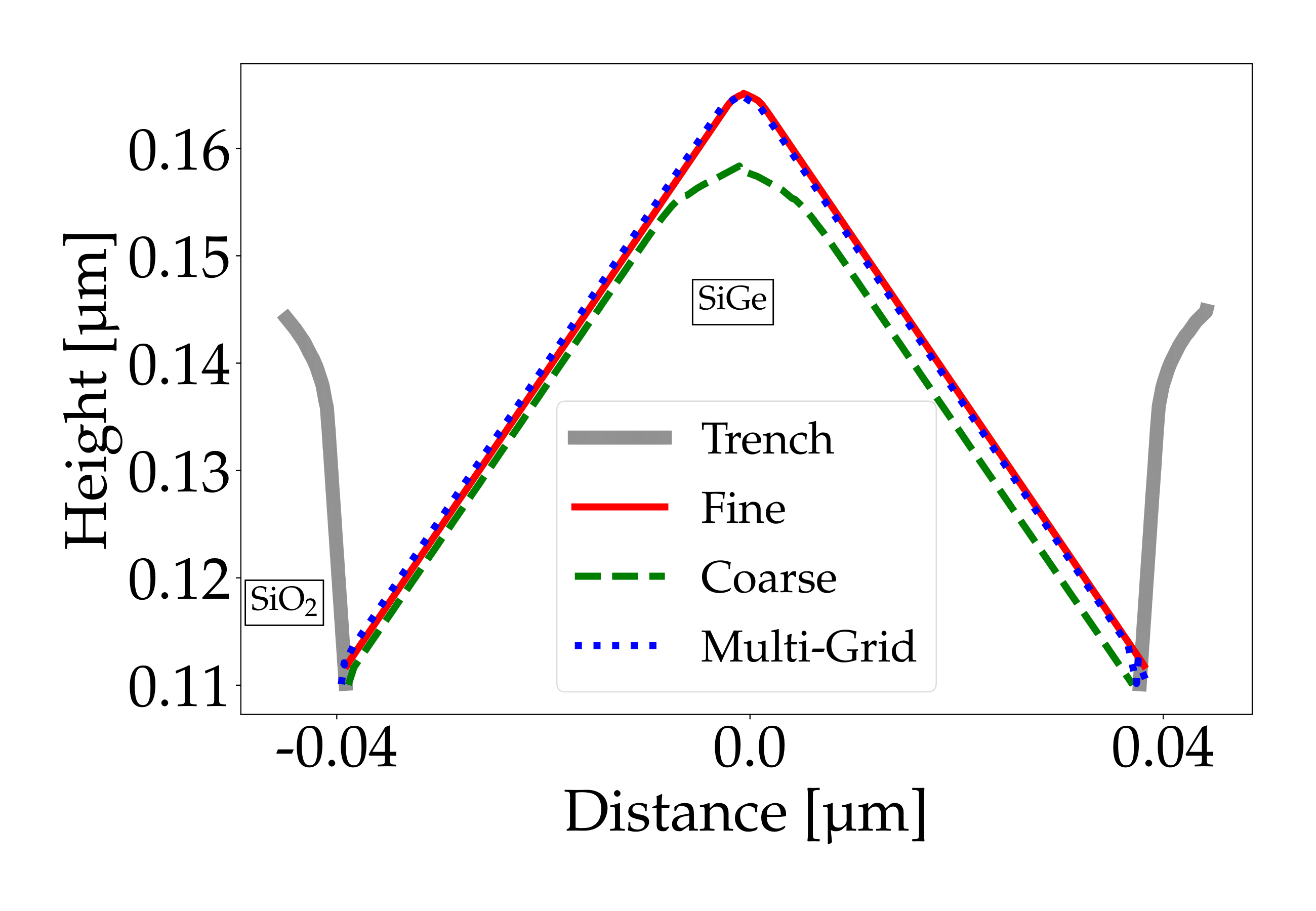
Fig. 2: Surface for the final simulation result of the SEG process after 47 SEG cycles using Coarse, Fine, and Multi-grid grid parameters. The error in the peak of the SiGe crystal using Coarse resolution is largest, since the grid resolution is not high enough to properly simulate the SEG process at this feature.
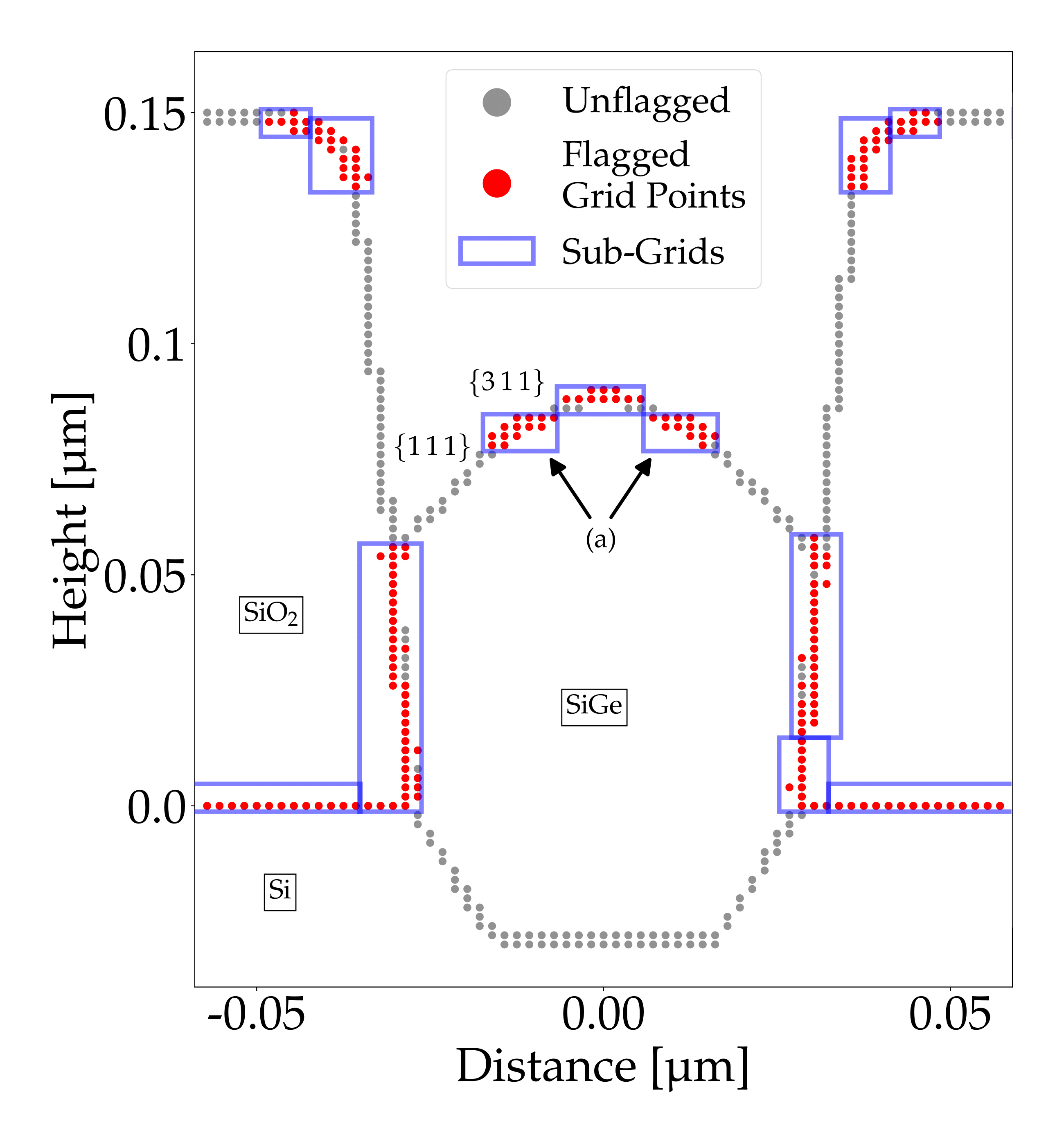
Fig. 3: Grid points near the level-set function for Grid 1 (i.e., base grid) of the simulation using Multi-grid grid parameters after 24 SEG cycles. The flagged grid points (red) and generated sub-grids (blue boxes) for this time step are shown. (a) indicates sub-grids over fine features that develop during the SEG process.