
 |
|
||||
BiographyFrâncio Souza Berti Rodrigues was born in 1991 in Caxias do Sul, Brazil. He received his Bachelor's degree in Engineering Physics from the Federal University of Rio Grande do Sul (BSc, 2015). Subsequently, he received his Master's Degree in Microelectronics Manufacturing from the same university (MSc, 2018). After finishing his studies, he worked in research and development for the packaging industry before joining the Institute for Microelectronics in September 2019. He is currently pursuing his doctoral degree, researching high performance numerical approaches for Technology CAD within the scope of the Christian Doppler Laboratory for High Performance TCAD. |
|||||
Feature-scale Modeling of Fluorocarbon Plasma Etching
The continuous development of semiconductor device performance demands ever-increasing progress in fabrication technologies. One of the key challenging fabrication steps is plasma etching — in particular, when considering dense structures with increasingly demanding high aspect ratios (HARs) and material selectivity constraints. Due to the intricacy of plasma etching, time-consuming empirical studies are required during the development of new fabrication approaches. Precise and efficient modeling of dry etching is thus needed to aid manufacturing progress by providing a virtual prototyping tool.
We have implemented a TCAD workflow for feature-scale etching into Silvaco’s process simulation tool Victory Process (Fig. 1). A bottom-up ray tracer is used to calculate the fluxes of chemical species into different geometries and source distributions. These fluxes serve as an input to a Langmuir set of coverage equations that describes the surface chemistry mechanisms. The coverage equations output the local etch or polymer deposition rates. The Langmuir set of equations takes into account sputtering etching, chemical etching, RIE etching, and polymer deposition mechanisms. A level-set engine applies the etch or deposition rates to the whole surface and updates the topography accordingly.
We apply the TCAD workflow to the via etching of SiO2 structures by Ar/C4F8, and we are able to reproduce a realistic via topography (Fig. 2). The etch rate for the entire procedure is 560nm/min, well inside the expected range of 500-600nm/min for the chosen parameters. Our mask etch rate of 80nm/min is also inside the expected range, and its faceting structure is expected for materials in which physical sputtering is the main etching mechanism. Fig. 3 depicts the etch rate evolution with time and via aspect ratio. The Aspect Ratio Dependent Etching (ARDE) phenomenon for this particular experiment is studied and shows that the etch rate falls below 500nm/min for aspect ratios larger than 7, representing a considerable increase in total etch time for higher aspect ratio via fabrication. This workflow can be extended to different materials and etching reactants, provide input for a device simulator, and is a quick and cost-effective tool to optimize plasma etching processes.
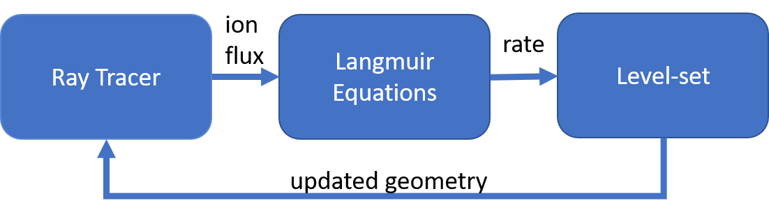
Fig. 1: Flow diagram of the TCAD workflow. The ray tracer evaluates the flux of incoming ions. The Langmuir model outputs the etch or deposition rates, and the level-set engine updates the feature shape.
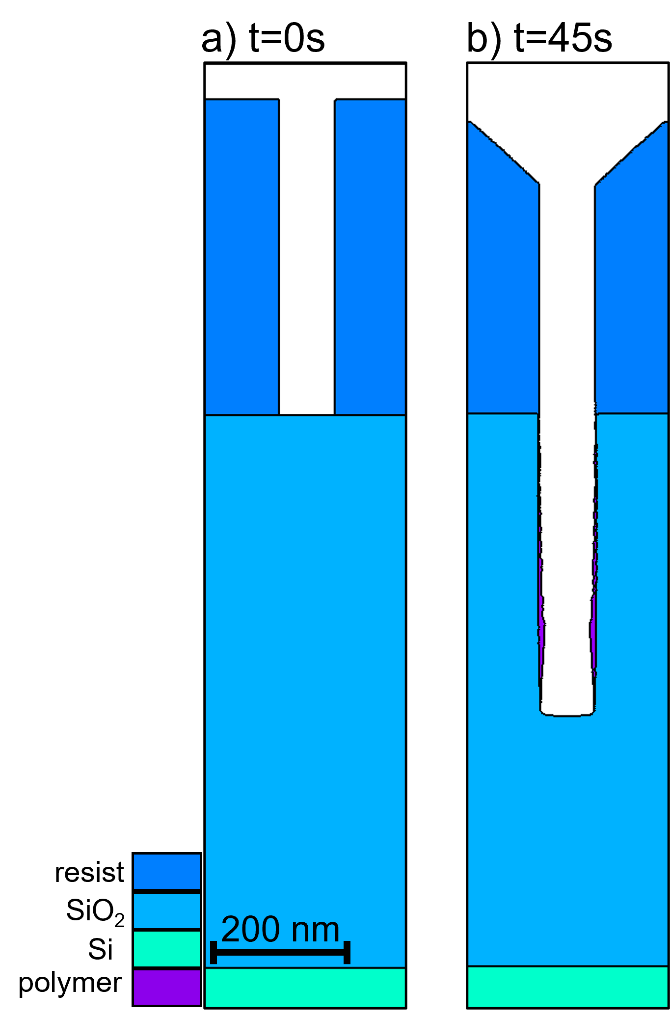
Fig. 2: a) Initial experimental setup with a 85nm opening and a resist height of 470nm. b) After 45s of etch time, the resist layer is thinner and exhibits faceting. The polymer layer, visible at the via sidewalls, enables the fabrication of highly anisotropic structures.
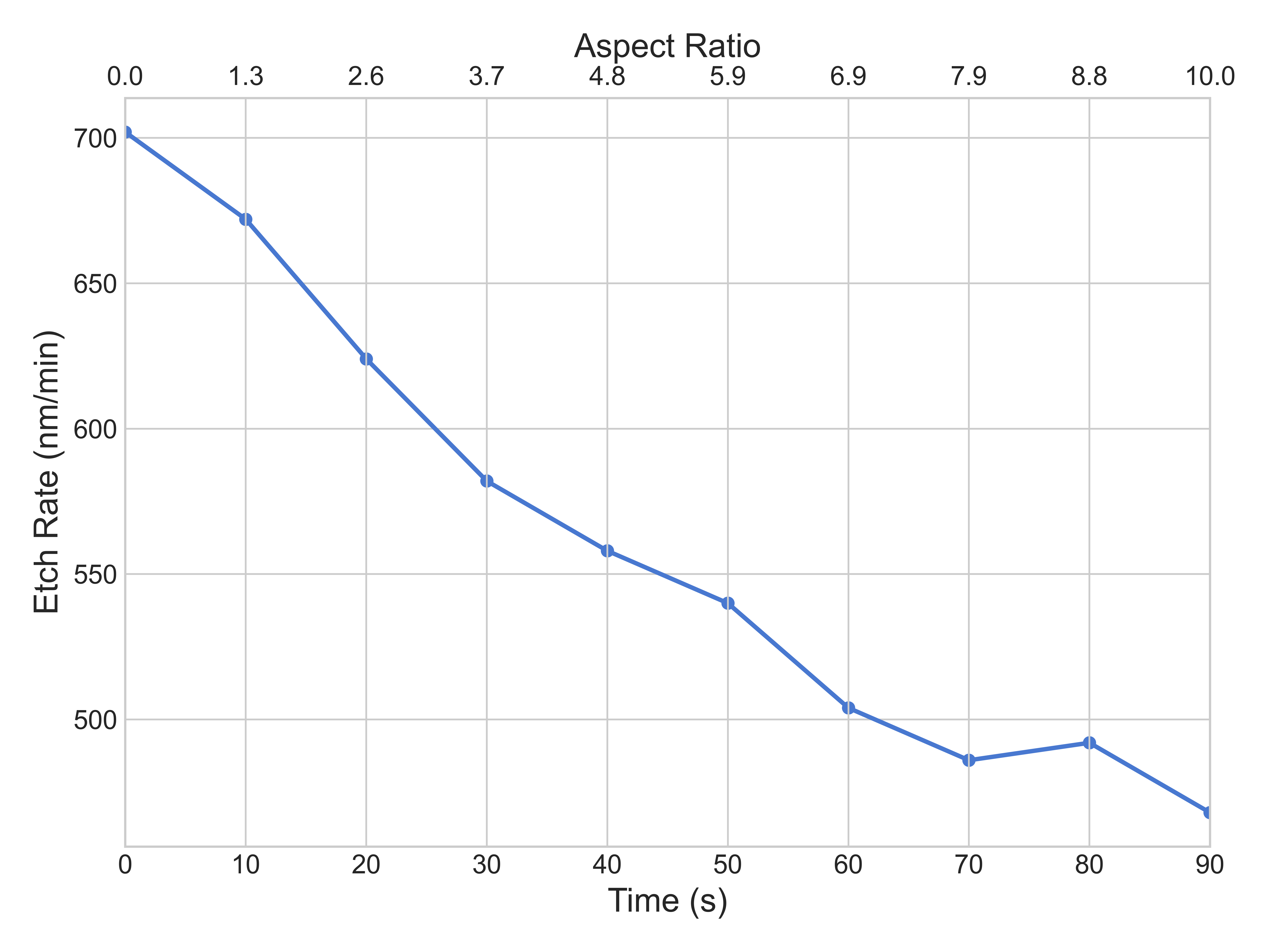
Fig. 3: Etch rate as a function of time and aspect ratio. Our average etch rate of 560nm/min is within the expected range of 500-600nm/min, and the ARDE lag effect is reproduced and characterized.